
- English
- Español
- Português
- русский
- Français
- 日本語
- Deutsch
- tiếng Việt
- Italiano
- Nederlands
- ภาษาไทย
- Polski
- 한국어
- Svenska
- magyar
- Malay
- বাংলা ভাষার
- Dansk
- Suomi
- हिन्दी
- Pilipino
- Türkçe
- Gaeilge
- العربية
- Indonesia
- Norsk
- تمل
- český
- ελληνικά
- український
- Javanese
- فارسی
- தமிழ்
- తెలుగు
- नेपाली
- Burmese
- български
- ລາວ
- Latine
- Қазақша
- Euskal
- Azərbaycan
- Slovenský jazyk
- Македонски
- Lietuvos
- Eesti Keel
- Română
- Slovenski
- मराठी
- Srpski језик

Silicon(Si) epitaxy preparation technology
2024-07-16
Silicon(Si) epitaxy preparation technology
What is epitaxial growth?
·Single crystal materials alone cannot meet the needs of the growing production of various semiconductor devices. At the end of 1959, a thin layer of single crystal material growth technology - epitaxial growth was developed.
Epitaxial growth is to grow a layer of material that meets the requirements on a single crystal substrate that has been carefully processed by cutting, grinding, and polishing under certain conditions. Since the grown single product layer is an extension of the substrate lattice, the grown material layer is called an epitaxial layer.
Classification by the properties of the epitaxial layer
·Homogeneous epitaxy: The epitaxial layer is the same as the substrate material, which maintains the consistency of the material and helps to achieve high-quality product structure and electrical properties.
·Heterogeneous epitaxy: The epitaxial layer is different from the substrate material. By selecting a suitable substrate, the growth conditions can be optimized and the application range of the material can be expanded, but the challenges brought by lattice mismatch and thermal expansion differences need to be overcome.
Classification by device position
Positive epitaxy: refers to the formation of an epitaxial layer on the substrate material during crystal growth, and the device is made on the epitaxial layer.
Reverse epitaxy: In contrast to positive epitaxy, the device is manufactured directly on the substrate, while the epitaxial layer is formed on the device structure.
Application differences: The application of the two in semiconductor manufacturing depends on the required material properties and device design requirements, and each is suitable for different process flows and technical requirements.
Classification by epitaxial growth method
· Direct epitaxy is a method of using heating, electron bombardment or external electric field to make the growing material atoms obtain enough energy, and directly migrate and deposit on the substrate surface to complete epitaxial growth, such as vacuum deposition, sputtering, sublimation, etc. However, this method has strict requirements on equipment. The resistivity and thickness of the film have poor repeatability, so it has not been used in silicon epitaxial production.
· Indirect epitaxy is the use of chemical reactions to deposit and grow epitaxial layers on the substrate surface, which is broadly called chemical vapor deposition (CVD). However, the thin film grown by CVD is not necessarily a single product. Therefore, strictly speaking, only CVD that grows a single film is epitaxial growth. This method has simple equipment, and the various parameters of the epitaxial layer are easier to control and have good repeatability. At present, silicon epitaxial growth mainly uses this method.
Other categories
·According to the method of transporting atoms of epitaxial materials to the substrate, it can be divided into vacuum epitaxy, gas phase epitaxy, liquid phase epitaxy(LPE), etc.
·According to the phase change process, epitaxy can be divided into gas phase epitaxy, liquid phase epitaxy, and solid phase epitaxy.
Problems solved by epitaxial process
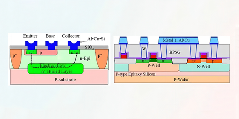
·When silicon epitaxial growth technology began, it was the time when silicon high-frequency and high-power transistor manufacturing encountered difficulties. From the perspective of transistor principle, to obtain high frequency and high power, the collector breakdown voltage must be high and the series resistance must be small, that is, the saturation voltage drop must be small. The former requires the resistivity of the collector area material to be high, while the latter requires the resistivity of the collector area material to be low, and the two are contradictory. If the series resistance is reduced by thinning the thickness of the collector area material, the silicon wafer will be too thin and fragile to be processed. If the resistivity of the material is reduced, it will contradict the first requirement. Epitaxial technology has successfully solved this difficulty.
Solution:
·Grow a high-resistivity epitaxial layer on a substrate with extremely low resistivity, and manufacture the device on the epitaxial layer. The high-resistivity epitaxial layer ensures that the tube has a high breakdown voltage, while the low-resistivity substrate reduces the resistance of the substrate and the saturation voltage drop, thus solving the contradiction between the two.
In addition, epitaxial technologies such as vapor phase epitaxy, liquid phase epitaxy, molecular beam epitaxy, and metal organic compound vapor phase epitaxy of 1-V family, 1-V family, and other compound semiconductor materials such as GaAs have also been greatly developed and have become indispensable process technologies for the manufacture of most microwave and optoelectronic devices.
In particular, the successful application of molecular beam and metal organic vapor phase epitaxy in ultra-thin layers, superlattices, quantum wells, strained superlattices, and atomic-level thin layer epitaxy has laid the foundation for the development of a new field of semiconductor research, "band engineering".
Characteristics of epitaxial growth
(1) High (low) resistance epitaxial layers can be grown epitaxially on low (high) resistance substrates.
(2) N(P) epitaxial layers can be grown on P(N) substrates to directly form PN junctions. There is no compensation problem when making PN junctions on single substrates by diffusion.
(3) Combined with mask technology, selective epitaxial growth can be carried out in designated areas, creating conditions for the production of integrated circuits and devices with special structures.
(4) The type and concentration of doping can be changed as needed during epitaxial growth. The concentration change can be abrupt or gradual.
(5) Ultra-thin layers of heterogeneous, multi-layered, multi-component compounds with variable components can be grown.
(6) Epitaxial growth can be carried out at a temperature below the melting point of the material. The growth rate is controllable, and epitaxial growth of atomic-scale thickness can be achieved.
Requirements for epitaxial growth
(1) The surface should be flat and bright, without surface defects such as bright spots, pits, fog stains and slip lines
(2) Good crystal integrity, low dislocation and stacking fault density. For silicon epitaxy, the dislocation density should be less than 1000/cm2, the stacking fault density should be less than 10/cm2, and the surface should remain bright after being corroded by chromic acid etching solution.
(3) The background impurity concentration of the epitaxial layer should be low and less compensation should be required. The raw material purity should be high, the system should be well sealed, the environment should be clean, and the operation should be strict to avoid the incorporation of foreign impurities into the epitaxial layer.
(4) For heterogeneous epitaxy, the composition of the epitaxial layer and the substrate should change suddenly (except for the requirement of slow composition change) and the mutual diffusion of the composition between the epitaxial layer and the substrate should be minimized.
(5) The doping concentration should be strictly controlled and evenly distributed so that the epitaxial layer has a uniform resistivity that meets the requirements. It is required that the resistivity of epitaxial wafers grown in different furnaces in the same furnace should be consistent.
(6) The thickness of the epitaxial layer should meet the requirements, with good uniformity and repeatability.
(7) After epitaxial growth on a substrate with a buried layer, the buried layer pattern distortion is very small.
(8) The diameter of the epitaxial wafer should be as large as possible to facilitate mass production of devices and reduce costs.
(9) The thermal stability of compound semiconductor epitaxial layers and heterojunction epitaxy is good.


