
- English
- Español
- Português
- русский
- Français
- 日本語
- Deutsch
- tiếng Việt
- Italiano
- Nederlands
- ภาษาไทย
- Polski
- 한국어
- Svenska
- magyar
- Malay
- বাংলা ভাষার
- Dansk
- Suomi
- हिन्दी
- Pilipino
- Türkçe
- Gaeilge
- العربية
- Indonesia
- Norsk
- تمل
- český
- ελληνικά
- український
- Javanese
- فارسی
- தமிழ்
- తెలుగు
- नेपाली
- Burmese
- български
- ລາວ
- Latine
- Қазақша
- Euskal
- Azərbaycan
- Slovenský jazyk
- Македонски
- Lietuvos
- Eesti Keel
- Română
- Slovenski
- मराठी
- Srpski језик


China Surface Treatment Technology Manufacturer, Supplier, Factory
- View as

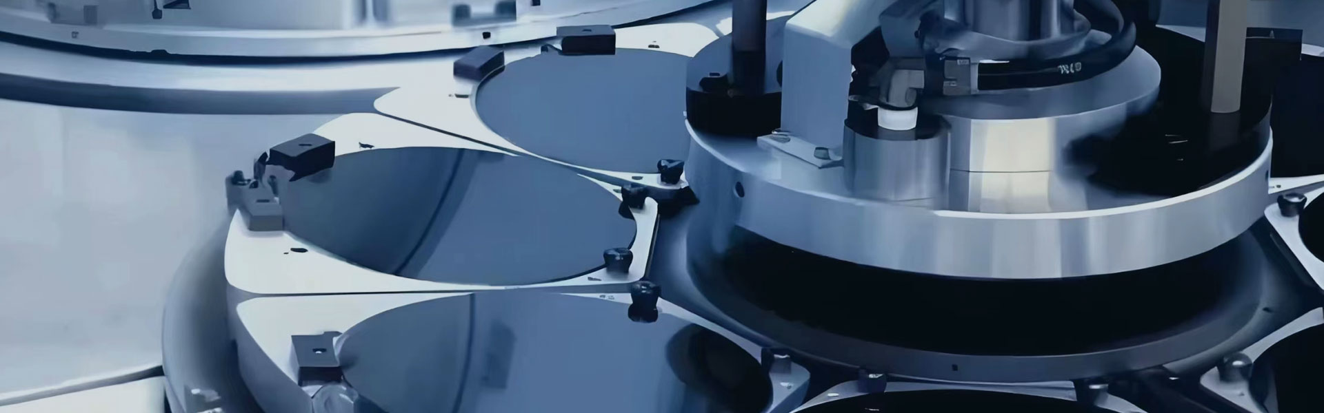
Physical Vapor Deposition
Vetek semiconductor Physical Vapor Deposition (PVD) is an advanced process technology widely used in surface treatment and thin film preparation. PVD technology uses physical methods to directly transform materials from solid or liquid to gas and form a thin film on the surface of the target substrate. This technology has the advantages of high precision, high uniformity and strong adhesion, and is widely used in semiconductors, optical devices, tool coatings and decorative coatings. Welcome to discuss with us!
Read MoreSend Inquiry
Thermal spraying technology MLCC capacitor
Vetek Semiconductor thermal spraying technology plays an extremely important role in the coating application of sintered crucibles for high-end multilayer ceramic capacitor (MLCC) materials. With the continuous miniaturization and high performance of electronic devices, the demand for thermal spraying technology MLCC capacitors is also growing rapidly, especially in high-end applications. In order to meet this demand, the crucibles used in the sintering process must have excellent high temperature resistance, corrosion resistance and good thermal conductivity, all of which can be achieved and improved by thermal spraying technology. Looking forward to setting up long term business with you.
Read MoreSend Inquiry
Semiconductor thermal spraying technology
Vetek Semiconductor Semiconductor thermal spraying technology is an advanced process that sprays materials in a molten or semi-molten state onto the surface of a substrate to form a coating. This technology is widely used in the field of semiconductor manufacturing, mainly used to create coatings with specific functions on the surface of the substrate, such as conductivity, insulation, corrosion resistance, and oxidation resistance. The main advantages of thermal spraying technology include high efficiency, controllable coating thickness, and good coating adhesion, making it particularly important in the semiconductor manufacturing process that requires high precision and reliability. Looking forward to your inquiry.
Read MoreSend Inquiry
MAX Phase Nanopowder
Veteksemi’s Semiconductor MAX phase nanopowder offers exceptional thermal and electrical properties, ideal for advanced electronics and materials science applications. With superior oxidation resistance and high-temperature stability, Veteksemi's nanopowder is the perfect solution for innovative semiconductor technologies.Welcome to inquiry us.
Read MoreSend Inquiry
As a professional Surface Treatment Technology manufacturer and supplier in China, we have our own factory. Whether you need customized services to meet the specific needs of your region or want to buy advanced and durable Surface Treatment Technology made in China, you can leave us a message.


