
- English
- Español
- Português
- русский
- Français
- 日本語
- Deutsch
- tiếng Việt
- Italiano
- Nederlands
- ภาษาไทย
- Polski
- 한국어
- Svenska
- magyar
- Malay
- বাংলা ভাষার
- Dansk
- Suomi
- हिन्दी
- Pilipino
- Türkçe
- Gaeilge
- العربية
- Indonesia
- Norsk
- تمل
- český
- ελληνικά
- український
- Javanese
- فارسی
- தமிழ்
- తెలుగు
- नेपाली
- Burmese
- български
- ລາວ
- Latine
- Қазақша
- Euskal
- Azərbaycan
- Slovenský jazyk
- Македонски
- Lietuvos
- Eesti Keel
- Română
- Slovenski
- मराठी
- Srpski језик

Exploratory application of 3D printing technology in the semiconductor industry
2024-07-19
In an era of rapid technological development, 3D printing, as an important representative of advanced manufacturing technology, is gradually changing the face of traditional manufacturing. With the continuous maturity of technology and the reduction of costs, 3D printing technology has shown broad application prospects in many fields such as aerospace, automobile manufacturing, medical equipment, and architectural design, and has promoted the innovation and development of these industries.
It is worth noting that the potential impact of 3D printing technology in the high-tech field of semiconductors is becoming increasingly prominent. As the cornerstone of the development of information technology, the precision and efficiency of semiconductor manufacturing processes affect the performance and cost of electronic products. Faced with the needs of high precision, high complexity and rapid iteration in the semiconductor industry, 3D printing technology, with its unique advantages, has brought unprecedented opportunities and challenges to semiconductor manufacturing, and has gradually penetrated into all links of the semiconductor industry chain, indicating that the semiconductor industry is about to usher in a profound change.
Therefore, analyzing and exploring the future application of 3D printing technology in the semiconductor industry will not only help us grasp the development pulse of this cutting-edge technology, but also provide technical support and reference for the upgrading of the semiconductor industry. This article analyzes the latest progress of 3D printing technology and its potential applications in the semiconductor industry, and looks forward to how this technology can promote the semiconductor manufacturing industry.
3D printing technology
3D printing is also known as additive manufacturing technology. Its principle is to build a three-dimensional entity by stacking materials layer by layer. This innovative production method subverts the traditional manufacturing "subtractive" or "equal material" processing mode, and can "integrate" molded products without mold assistance. There are many types of 3D printing technologies, and each technology has its own advantages.
According to the molding principle of 3D printing technology, there are mainly four types.
✔ Photocuring technology is based on the principle of ultraviolet polymerization. Liquid photosensitive materials are cured by ultraviolet light and stacked layer by layer. At present, this technology can form ceramics, metals, and resins with high molding precision. It can be used in the fields of medical, art, and aviation industry.
✔ Fused deposition technology, through the computer-driven print head to heat and melt the filament, and extrude it according to a specific shape trajectory, layer by layer, and can form plastic and ceramic materials.
✔ Slurry direct writing technology uses high-viscosity slurry as ink material, which is stored in the barrel and connected to the extrusion needle, and installed on a platform that can complete three-dimensional movement under computer control. Through mechanical pressure or pneumatic pressure, the ink material is pushed out of the nozzle to continuously extrude on the substrate to form, and then the corresponding post-processing (volatile solvent, thermal curing, light curing, sintering, etc.) is carried out according to the material properties to obtain the final three-dimensional component. At present, this technology can be applied to the fields of bioceramics and food processing.
✔Powder bed fusion technology can be divided into laser selective melting technology (SLM) and laser selective sintering technology (SLS). Both technologies use powder materials as processing objects. Among them, the laser energy of SLM is higher, which can make the powder melt and solidify in a short time. SLS can be divided into direct SLS and indirect SLS. The energy of direct SLS is higher, and the particles can be directly sintered or melted to form bonding between particles. Therefore, direct SLS is similar to SLM. The powder particles undergo rapid heating and cooling in a short time, which makes the molded block have large internal stress, low overall density, and poor mechanical properties; the laser energy of indirect SLS is lower, and the binder in the powder is melted by the laser beam and the particles are bonded. After the forming is completed, the internal binder is removed by thermal degreasing, and finally sintering is performed. Powder bed fusion technology can form metals and ceramics and is currently used in the aerospace and automotive manufacturing fields.
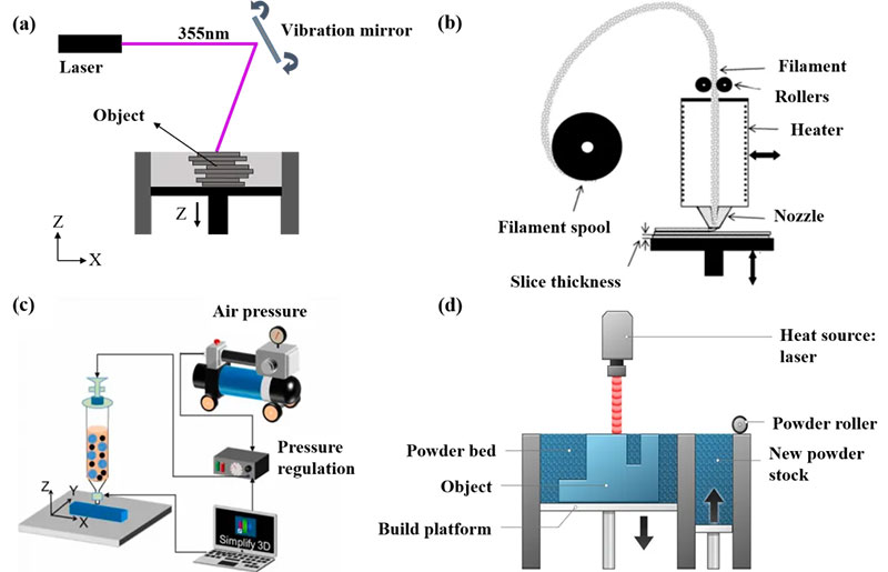
Figure 1 (a) Photocuring technology; (b) Fused deposition technology; (c) Slurry direct writing technology; (d) Powder bed fusion technology [1, 2]
With the continuous development of 3D printing technology, its advantages are constantly being demonstrated from prototyping to final products. First, in terms of the freedom of product structure design, the most significant advantage of 3D printing technology is that it can directly manufacture complex structures of workpieces. Next, in terms of the material selection of the molding object, 3D printing technology can print a variety of materials, including metals, ceramics, polymer materials, etc. In terms of the manufacturing process, 3D printing technology has a high degree of flexibility and can adjust the manufacturing process and parameters according to actual needs.
Semiconductor industry
The semiconductor industry plays a vital role in modern science and technology and economy, and its importance is reflected in many aspects. Semiconductors are used to build miniaturized circuits, which enable devices to perform complex computing and data processing tasks. And as an important pillar of the global economy, the semiconductor industry provides a large number of jobs and economic benefits for many countries. It not only directly promoted the development of the electronics manufacturing industry, but also led to the growth of industries such as software development and hardware design. In addition, in the military and defense fields, semiconductor technology is crucial for key equipment such as communication systems, radars, and satellite navigation, ensuring national security and military advantages.
Chart 2 "14th Five-Year Plan" (excerpt) [3]
Therefore, the current semiconductor industry has become an important symbol of national competitiveness, and all countries are actively developing it. my country's "14th Five-Year Plan" proposes to focus on supporting various key "bottleneck" links in the semiconductor industry, mainly including advanced processes, key equipment, third-generation semiconductors and other fields.
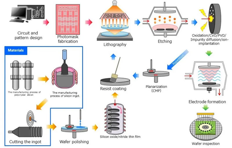
Chart 3 Semiconductor chip processing process [4]
The manufacturing process of semiconductor chips is extremely complex. As shown in Figure 3, it mainly includes the following key steps: wafer preparation, lithography, etching, thin film deposition, ion implantation, and packaging testing. Each process requires strict control and precise measurement. Problems in any link may cause damage to the chip or performance degradation. Therefore, semiconductor manufacturing has very high requirements for equipment, processes and personnel.
Although traditional semiconductor manufacturing has achieved great success, there are still some limitations: First, semiconductor chips are highly integrated and miniaturized. With the continuation of Moore's Law (Figure 4), the integration of semiconductor chips continues to increase, the size of components continues to shrink, and the manufacturing process needs to ensure extremely high precision and stability.
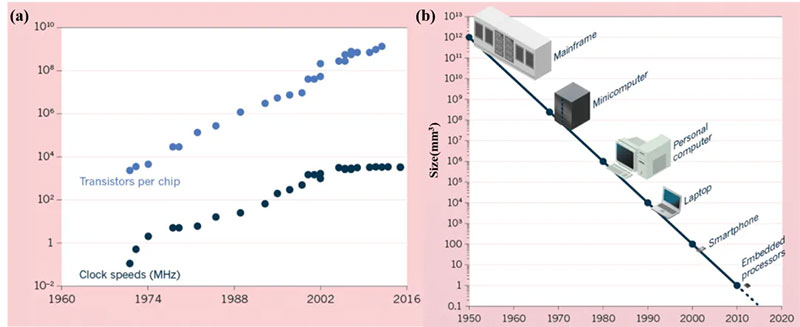
Figure 4 (a) The number of transistors in a chip continues to increase over time; (b) The chip size continues to shrink [5]
In addition, the complexity and cost control of the semiconductor manufacturing process. The semiconductor manufacturing process is complex and relies on precision equipment, and each link needs to be accurately controlled. The high equipment cost, material cost and R&D cost make the manufacturing cost of semiconductor products high. Therefore, it is necessary to continue to explore and reduce costs while ensuring product yield.
At the same time, the semiconductor manufacturing industry needs to respond quickly to market demand. With the rapid changes in market demand. The traditional manufacturing model has the problems of long cycle and poor flexibility, which makes it difficult to meet the market's rapid iteration of products. Therefore, a more efficient and flexible manufacturing method has also become the development direction of the semiconductor industry.
Application of 3D printing in the semiconductor industry
In the semiconductor field, 3D printing technology has also continuously demonstrated its application.
First, 3D printing technology has a high degree of freedom in structural design and can achieve "integrated" molding, which means that more sophisticated and complex structures can be designed. Figure 5 (a), 3D System optimizes the internal heat dissipation structure through artificial auxiliary design, improves the thermal stability of the wafer stage, reduces the thermal stabilization time of the wafer, and improves the yield and efficiency of chip production. There are also complex pipelines inside the lithography machine. Through 3D printing, complex pipeline structures can be "integrated" to reduce the use of hoses and optimize the gas flow in the pipeline, thereby reducing the negative impact of mechanical interference and vibration and improving the stability of the chip processing process.
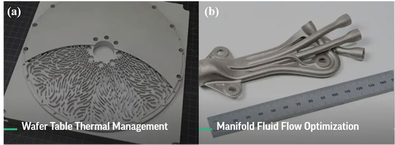
Figure 5 3D System uses 3D printing to form parts (a) lithography machine wafer stage; (b) manifold pipeline [6]
In terms of material selection, 3D printing technology can realize materials that are difficult to form by traditional processing methods. Silicon carbide materials have high hardness and high melting point. Traditional processing methods are difficult to form and have a long production cycle. The formation of complex structures requires mold-assisted processing. Sublimation 3D has developed an independent dual-nozzle 3D printer UPS-250 and prepared silicon carbide crystal boats. After reaction sintering, the product density is 2.95~3.02g/cm3.
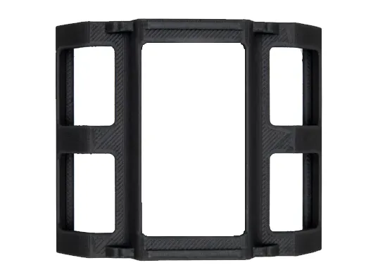
Figure 6 Silicon carbide crystal boat[7]
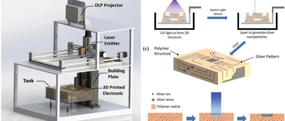
Figure 7 (a) 3D co-printing equipment; (b) UV light is used to construct three-dimensional structures, and laser is used to generate silver nanoparticles; (c) Principle of 3D co-printing electronic components[8]
The traditional electronic product process is complex, and multiple process steps are required from raw materials to finished products. Xiao et al.[8] used 3D co-printing technology to selectively construct body structures or embed conductive metals on free-form surfaces to manufacture 3D electronic devices. This technology only involves one printing material, which can be used to build polymer structures through UV curing, or to activate metal precursors in photosensitive resins through laser scanning to produce nano-metal particles to form conductive circuits. In addition, the resulting conductive circuit exhibits an excellent resistivity as low as about 6.12µΩm. By adjusting the material formula and processing parameters, the resistivity can be further controlled between 10-6 and 10Ωm. It can be seen that 3D co-printing technology solves the challenge of multi-material deposition in traditional manufacturing and opens up a new path for manufacturing 3D electronic products.
Chip packaging is a key link in semiconductor manufacturing. Traditional packaging technology also has problems such as complex process, failure of thermal management, and stress caused by mismatch of thermal expansion coefficients between materials, which leads to packaging failure. 3D printing technology can simplify the manufacturing process and reduce costs by directly printing the packaging structure. Feng et al. [9] prepared phase change electronic packaging materials and combined them with 3D printing technology to package chips and circuits. The phase change electronic packaging material prepared by Feng et al. has a high latent heat of 145.6 J/g and has significant thermal stability at a temperature of 130°C. Compared with traditional electronic packaging materials, its cooling effect can reach 13°C.
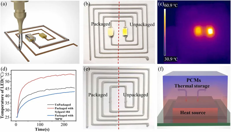
Figure 8 Schematic diagram of using 3D printing technology to accurately encapsulate circuits with phase change electronic materials; (b) The LED chip on the left has been encapsulated with phase change electronic packaging materials, and the LED chip on the right has not been encapsulated; (c) Infrared images of LED chips with and without encapsulation; (d) Temperature curves under the same power and different packaging materials; (e) Complex circuit without LED chip packaging diagram; (f) Schematic diagram of heat dissipation of phase change electronic packaging materials [9]
Challenges of 3D printing technology in the semiconductor industry
Although 3D printing technology has shown great potential in the semiconductor industry. However, there are still many challenges.
In terms of molding accuracy, the current 3D printing technology can achieve an accuracy of 20μm, but it is still difficult to meet the high standards of semiconductor manufacturing. In terms of material selection, although 3D printing technology can form a variety of materials, the molding difficulty of some materials with special properties (silicon carbide, silicon nitride, etc.) is still relatively high. In terms of production cost, 3D printing performs well in small-batch customized production, but its production speed is relatively slow in large-scale production, and the equipment cost is high, which makes it difficult to meet the needs of large-scale production. Technically, although 3D printing technology has achieved certain development results, it is still an emerging technology in some fields and requires further research and development and improvement to improve its stability and reliability.


