- English
- Español
- Português
- русский
- Français
- 日本語
- Deutsch
- tiếng Việt
- Italiano
- Nederlands
- ภาษาไทย
- Polski
- 한국어
- Svenska
- magyar
- Malay
- বাংলা ভাষার
- Dansk
- Suomi
- हिन्दी
- Pilipino
- Türkçe
- Gaeilge
- العربية
- Indonesia
- Norsk
- تمل
- český
- ελληνικά
- український
- Javanese
- فارسی
- தமிழ்
- తెలుగు
- नेपाली
- Burmese
- български
- ລາວ
- Latine
- Қазақша
- Euskal
- Azərbaycan
- Slovenský jazyk
- Македонски
- Lietuvos
- Eesti Keel
- Română
- Slovenski
- मराठी
- Srpski језик
China Porous SiC Manufacturer, Supplier, Factory
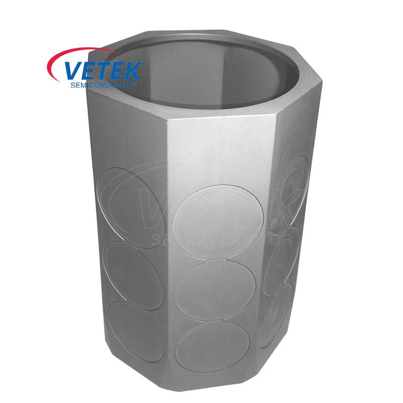
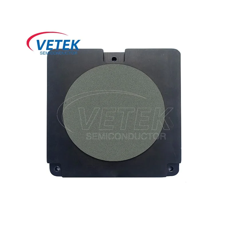
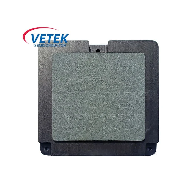
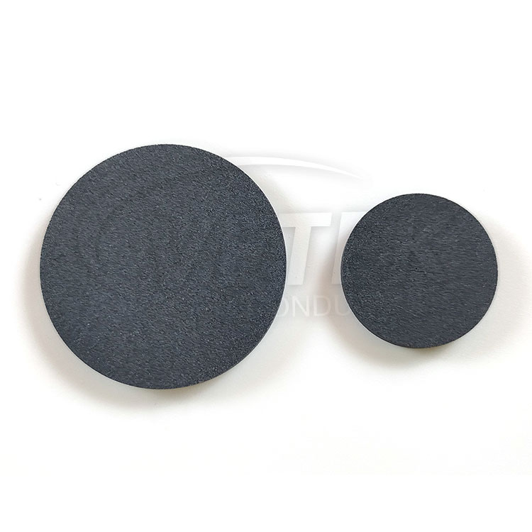
VeTek semiconductor is a leading manufacturer of Porous SiC ceramics for the semiconductor industry. Passed ISO9001, VeTek Semiconductor has good control on quality. VeTek Semiconductor has always been committed to becoming an innovator and leader in the porous SiC ceramic industry.
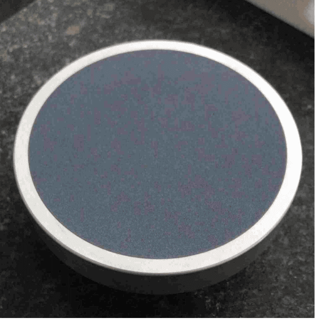
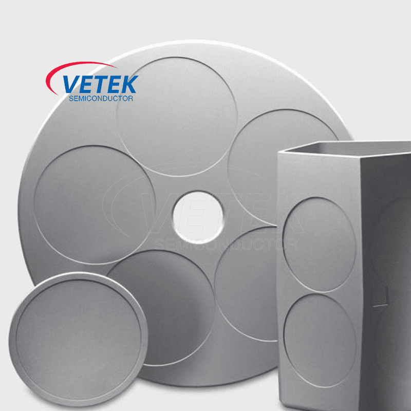
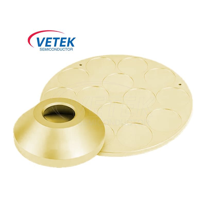
Porous SiC Ceramic Disc
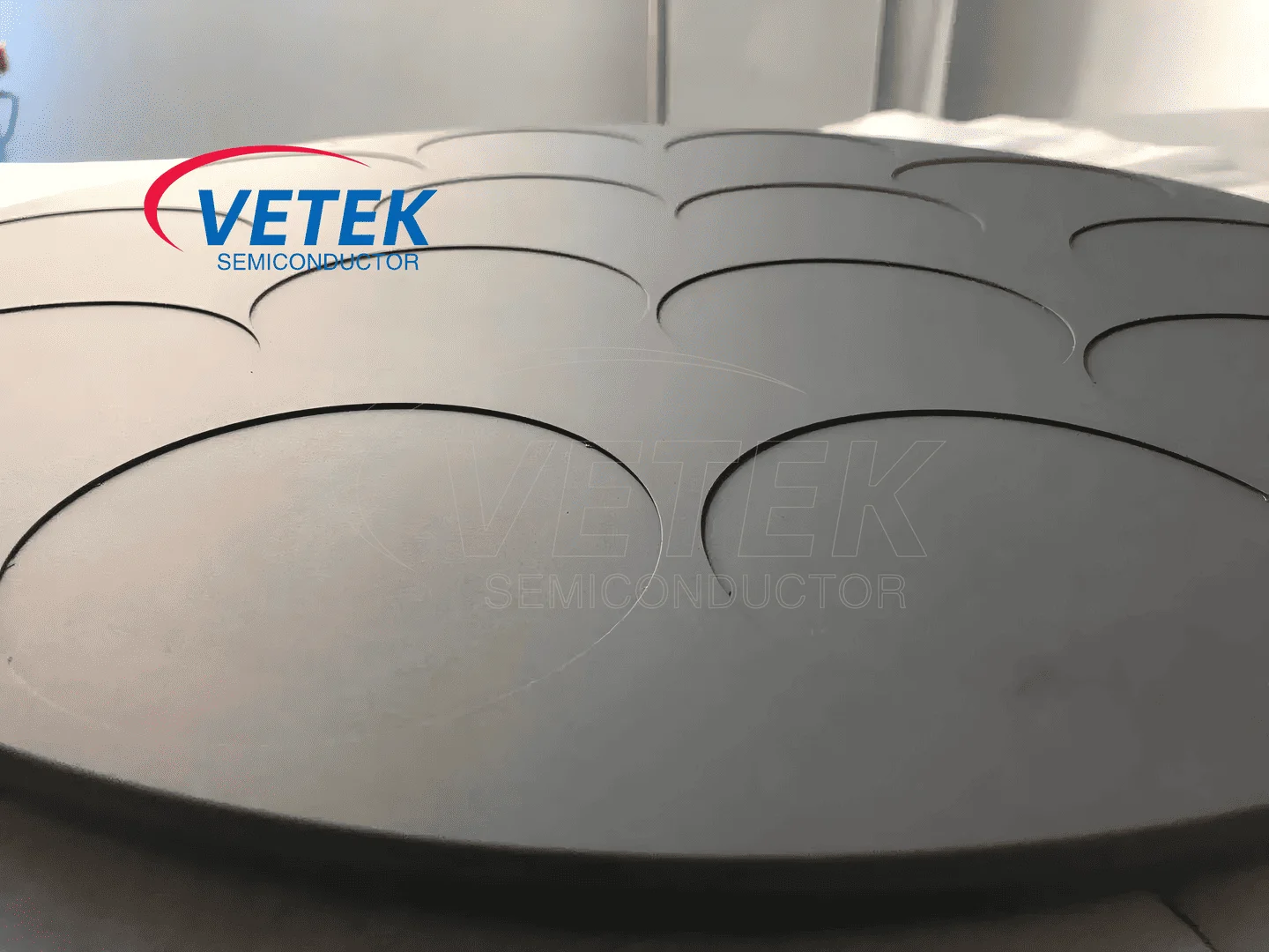
Porous SiC ceramics are ceramic material that are fired at high temperatures and have a large number of interconnected or closed pores inside. It is also known as a microporous vacuum suction cup, with pore sizes ranging from 2 to 100um.
Porous SiC ceramics have been widely used in metallurgy, chemical industry, environmental protection, biology, semiconductor and other fields. Porous SiC ceramics can be prepared by foaming method, sol gel method, tape casting method, solid sintering method and impregnation pyrolysis method.
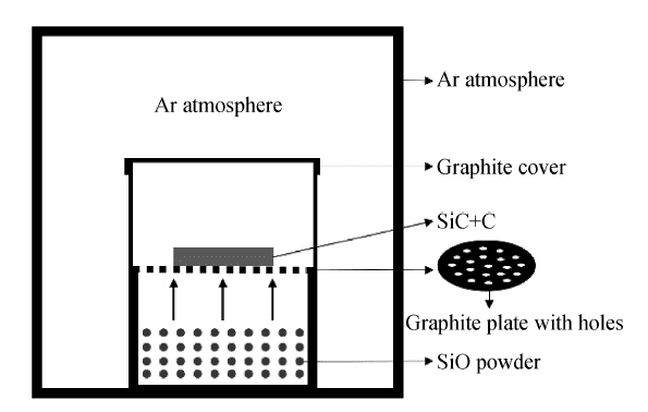
Preparation of porous SiC ceramics by sintering method
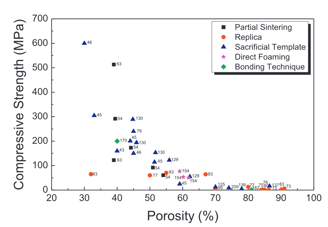
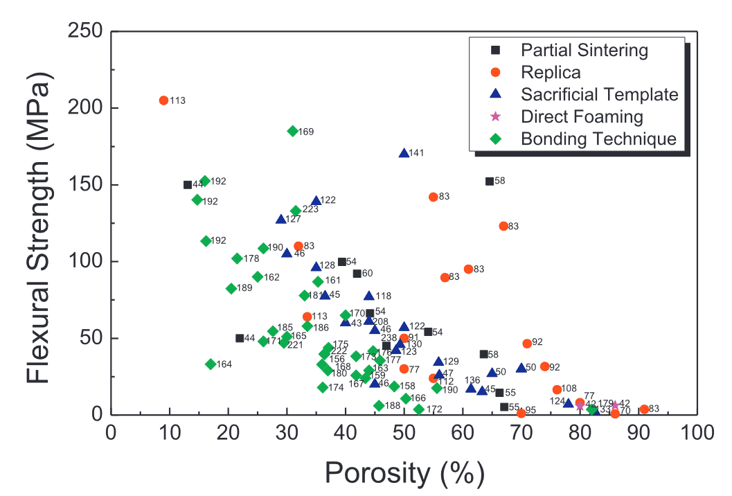
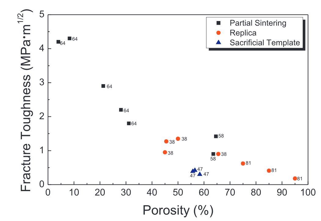
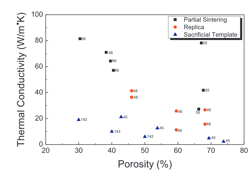
Properties of porous silicon carbide ceramics prepared by different methods as a function of porosity
![]()
porous SiC ceramics Suction Cups in Semiconductor Wafer Fabrication
VeTek Semiconductor's porous SiC ceramics play the role of clamping and carrying wafers in semiconductor production. They are dense and uniform, high in strength, good in air permeability, and uniform in adsorption.
They effectively address many difficult problems such as wafer indentation and chip electrostatic breakdown, and help achieve the processing of extremely high-quality wafers.
Working diagram of porous SiC ceramics:
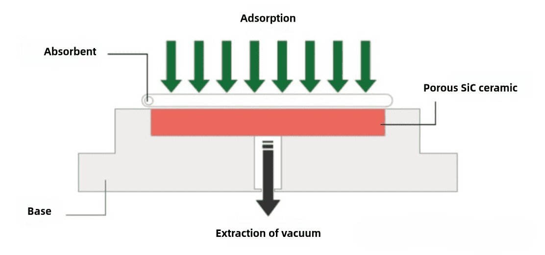
Working principle of porous SiC ceramics: The silicon wafer is fixed by the vacuum adsorption principle. During processing, the small holes on the porous SiC ceramics are used to extract the air between the silicon wafer and the ceramic surface, so that the silicon wafer and the ceramic surface are at low pressure, thereby fixing the silicon wafer.
After processing, plasma water flows out of the holes to prevent the silicon wafer from adhering to the ceramic surface, and at the same time, the silicon wafer and the ceramic surface are cleaned.
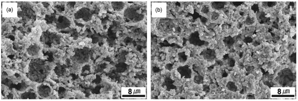
Microstructure of the porous SiC ceramics
Highlight advantages and features:
●High temperature resistance
●Resistance to wear
●Chemical resistance
●High mechanical strength
●Easy to regenerate
●Excellent thermal shock resistance
item
unit
porous SiC ceramics
Pore diameter
um
10~30
Density
g/cm3
1.2~1.3
Surface roughness
um
2.5~3
Air absorption value
KPA
-45
Flexural strength
MPa
30 Dielectric constant
1MHz
33 Thermal conductivity
W/(m·K)
60~70
There are several high requirements for porous SiC ceramics:
1. Strong vacuum adsorption
2. Flatness is very important, otherwise there will be problems during operation
3. No deformation and no metal impurities
Therefore, the Air absorption value of VeTek Semiconductor's porous SiC ceramics reaches -45KPA. At the same time, they are tempered at 1200℃ for 1.5 hours before leaving the factory to remove impurities and are packaged in vacuum bags.
Porous SiC ceramics are widely used in wafer processing technology, transfer and other links. They have made great achievements in bonding, dicing, mounting, polishing and other links.
- View as
Porous SiC Vacuum Chuck
As a professional Porous SiC Vacuum Chuck manufacturer and supplier in China, Vetek Semiconductor's Porous SiC Vacuum Chuck is widely used in key components of semiconductor manufacturing equipment, especially when it comes to CVD and PECVD processes. Vetek Semiconductor specializes in manufacturing and supplying high-performance Porous SiC Vacuum Chuck. Welcome your further inquiries.
Read MoreSend InquiryPorous Ceramic Vacuum Chuck
As a professional Porous Ceramic Vacuum Chuck manufacturer and supplier in China, Vetek Semiconductor's Porous Ceramic Vacuum Chuck is made of silicon carbide ceramic (SiC) material, which has excellent high temperature resistance, chemical stability and mechanical strength. It is an indispensable core component in the semiconductor manufacturing process. Welcome your further inquiries.
Read MoreSend InquiryPorous SiC Ceramic Chuck
Vetek Semiconductor offers Porous SiC Ceramic Chuck widely used in wafer processing technology, transfer and other links, suitable for bonding, scribing, patch, polishing and other links, laser processing. Our Porous SiC Ceramic Chuck has Ultra-strong vacuum adsorption, high flatness and high purity meet the needs of most semiconductor industries.Welcome to inquiry us.
Read MoreSend Inquiry
