- English
- Español
- Português
- русский
- Français
- 日本語
- Deutsch
- tiếng Việt
- Italiano
- Nederlands
- ภาษาไทย
- Polski
- 한국어
- Svenska
- magyar
- Malay
- বাংলা ভাষার
- Dansk
- Suomi
- हिन्दी
- Pilipino
- Türkçe
- Gaeilge
- العربية
- Indonesia
- Norsk
- تمل
- český
- ελληνικά
- український
- Javanese
- فارسی
- தமிழ்
- తెలుగు
- नेपाली
- Burmese
- български
- ລາວ
- Latine
- Қазақша
- Euskal
- Azərbaycan
- Slovenský jazyk
- Македонски
- Lietuvos
- Eesti Keel
- Română
- Slovenski
- मराठी
- Srpski језик
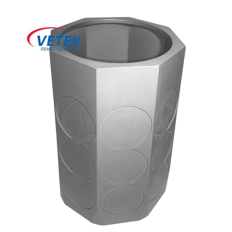
Crucible for Monocrystalline Silicon
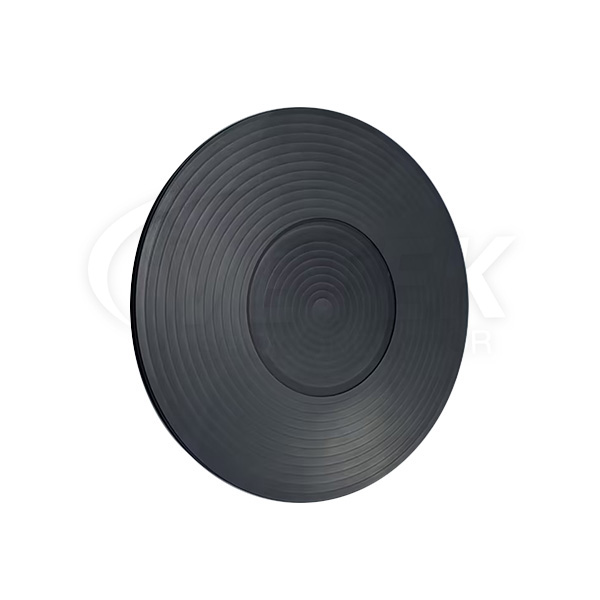
Vetek Semiconductor Crucible for Monocrystalline Silicon are essential for achieving single-crystal growth, a cornerstone of semiconductor device manufacturing. These crucibles are meticulously designed to meet the rigorous standards of the semiconductor industry, ensuring peak performance and efficiency in all applications. At Vetek Semiconductor, we are dedicated to manufacturing and supplying high-performance crucibles for crystal growth that combine quality with cost-efficiency.
Send Inquiry
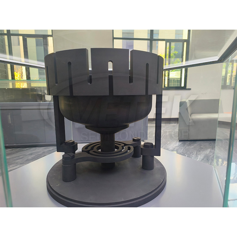
In the CZ (Czochralski) method, a single crystal is grown by bringing a monocrystalline seed into contact with molten polycrystalline silicon. The seed is gradually pulled upward while being rotated slowly. In this process, a significant number of graphite parts are used, making it the method that employs the highest quantity of graphite components in silicon semiconductor manufacturing.
The right picture provides a schematic representation of a silicon single-crystal manufacturing furnace based on the CZ method.
Vetek Semiconductor's Crucible for Monocrystalline Silicon provide a stable and controlled environment crucial for the precise formation of semiconductor crystals. They are instrumental in growing monocrystalline silicon ingots using advanced techniques such as the Czochralski process and float-zone methods, which are vital for producing high-quality materials for electronic devices.
Engineered for outstanding thermal stability, chemical corrosion resistance, and minimal thermal expansion, these crucibles ensure durability and robustness. They are designed to withstand harsh chemical environments without compromising structural integrity or performance, thereby extending the crucible's lifespan and maintaining consistent performance over prolonged use.
The unique composition of Vetek Semiconductor Crucibles for monocrystalline silicon enables them to endure the extreme conditions of high-temperature processing. This guarantees exceptional thermal stability and purity, which are critical for semiconductor processing. The composition also facilitates efficient heat transfer, promoting uniform crystallization and minimizing thermal gradients within the silicon melt.
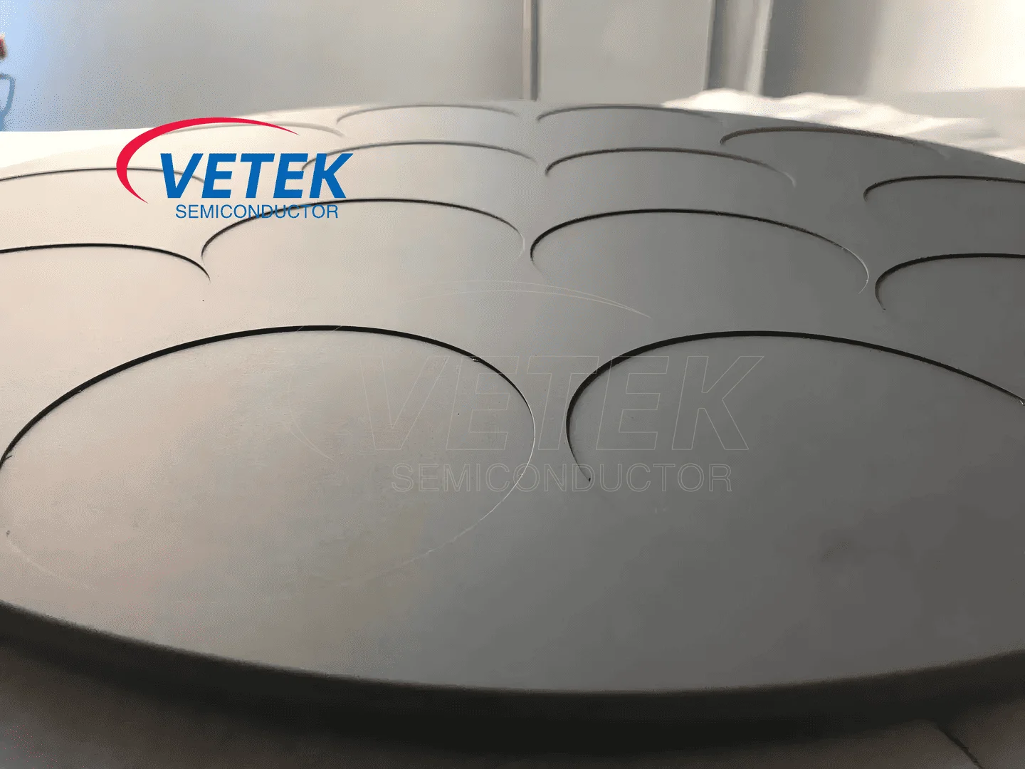
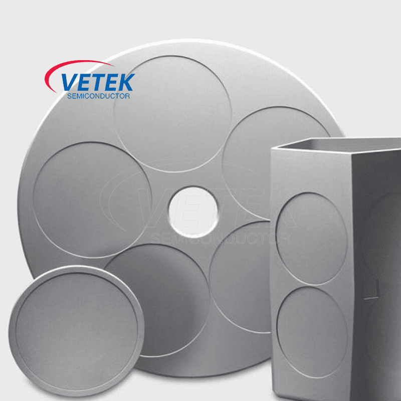
Advantages of our SiC Coating Susceptor:
✔ Base Material Protection: The CVD SiC coating acts as a protective layer during the epitaxial process, effectively shielding the base material from erosion and damage caused by the external environment. This protective measure greatly extends the service life of the equipment.
✔ Excellent Thermal Conductivity: Our CVD SiC coating possesses outstanding thermal conductivity, efficiently transferring heat from the base material to the coating surface. This enhances thermal management efficiency during epitaxy, ensuring optimal operating temperatures for the equipment.
✔ Improved Film Quality: The CVD SiC coating provides a flat and uniform surface, creating an ideal foundation for film growth. It reduces defects resulting from lattice mismatch, enhances the crystallinity and quality of the epitaxial film, and ultimately improves its performance and reliability.
Choose our SiC Coating Susceptor for your epitaxial wafer production needs, and benefit from enhanced protection, superior thermal conductivity, and improved film quality. Trust in VeTek Semiconductor's innovative solutions to drive your success in the semiconductor industry.
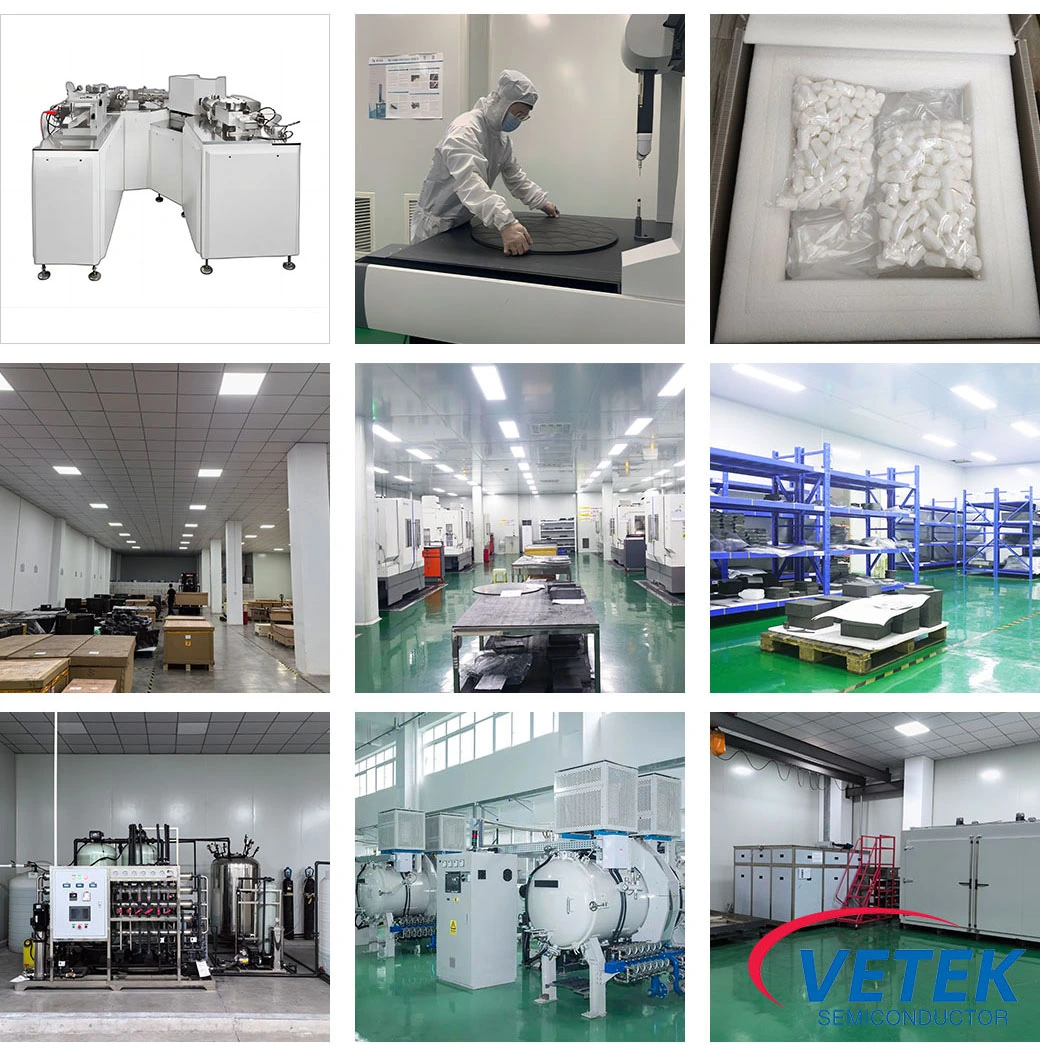
VeTekSemi Crucible for Monocrystalline Silicon Production shops:
