
- English
- Español
- Português
- русский
- Français
- 日本語
- Deutsch
- tiếng Việt
- Italiano
- Nederlands
- ภาษาไทย
- Polski
- 한국어
- Svenska
- magyar
- Malay
- বাংলা ভাষার
- Dansk
- Suomi
- हिन्दी
- Pilipino
- Türkçe
- Gaeilge
- العربية
- Indonesia
- Norsk
- تمل
- český
- ελληνικά
- український
- Javanese
- فارسی
- தமிழ்
- తెలుగు
- नेपाली
- Burmese
- български
- ລາວ
- Latine
- Қазақша
- Euskal
- Azərbaycan
- Slovenský jazyk
- Македонски
- Lietuvos
- Eesti Keel
- Română
- Slovenski
- मराठी
- Srpski језик


Semiconductor thermal spraying technology
Vetek Semiconductor Semiconductor thermal spraying technology is an advanced process that sprays materials in a molten or semi-molten state onto the surface of a substrate to form a coating. This technology is widely used in the field of semiconductor manufacturing, mainly used to create coatings with specific functions on the surface of the substrate, such as conductivity, insulation, corrosion resistance, and oxidation resistance. The main advantages of thermal spraying technology include high efficiency, controllable coating thickness, and good coating adhesion, making it particularly important in the semiconductor manufacturing process that requires high precision and reliability. Looking forward to your inquiry.
Send Inquiry
Product Description
Semiconductor thermal spraying technology is an advanced process that sprays materials in a molten or semi-molten state onto the surface of a substrate to form a coating. This technology is widely used in the field of semiconductor manufacturing, mainly used to create coatings with specific functions on the surface of the substrate, such as conductivity, insulation, corrosion resistance, and oxidation resistance. The main advantages of thermal spraying technology include high efficiency, controllable coating thickness, and good coating adhesion, making it particularly important in the semiconductor manufacturing process that requires high precision and reliability.
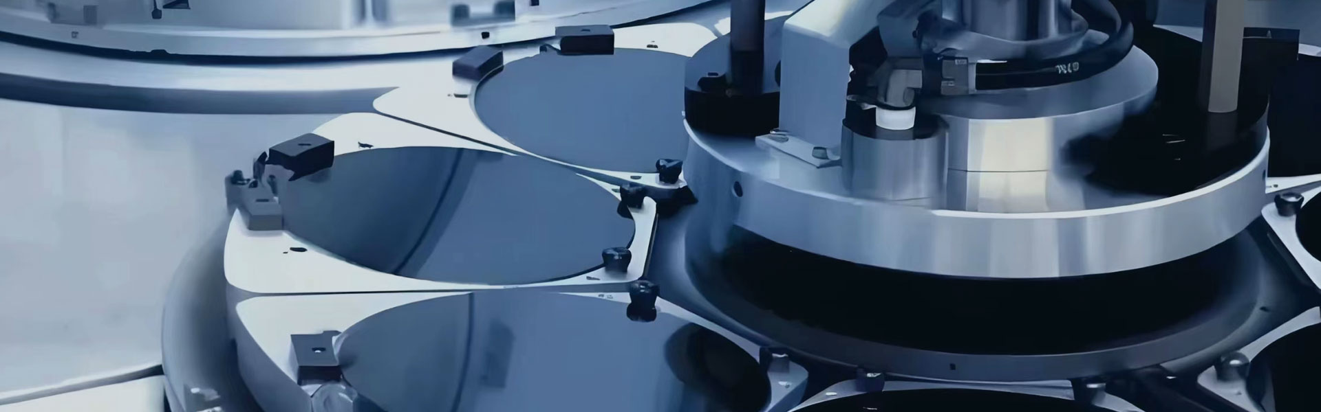
Application of thermal spraying technology in semiconductors
Plasma beam etching (dry etching)
Usually refers to the use of glow discharge to generate plasma active particles containing charged particles such as plasma and electrons and highly chemically active neutral atoms and molecules and free radicals, which diffuse to the part to be etched, react with the etched material, form volatile products and are removed, thereby completing the etching technology of pattern transfer. It is an irreplaceable process for realizing the high-fidelity transfer of fine patterns from photolithography templates to wafers in the production of ultra-large-scale integrated circuits.
A large number of active free radicals such as Cl and F will be generated. When they etch semiconductor devices, they corrode the inner surfaces of other parts of the equipment, including aluminum alloys and ceramic structural parts. This strong erosion produces a large number of particles, which not only requires frequent maintenance of production equipment, but also causes failure of the etching process chamber and damage to the device in severe cases.
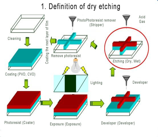
Y2O3 is a material with very stable chemical and thermal properties. Its melting point is far above 2400℃. It can remain stable in a strong corrosive environment. Its resistance to plasma bombardment can greatly extend the service life of components and reduce particles in the etching chamber.
The mainstream solution is to spray high-purity Y2O3 coating to protect the etching chamber and other key components.
Hot Tags: Semiconductor thermal spraying technology, China, Manufacturer, Supplier, Factory, Customized, Buy, Advanced, Durable, Made in China
Product Tag
Related Category
Tantalum Carbide Coating
Silicon Carbide Coating
Special Graphite
Carbon Fiber
Silicon Carbide Ceramics
Other Semiconductor Ceramics
Wafer
Surface Treatment Technology
Technical Service
Send Inquiry
Please feel free to give your inquiry in the form below. We will reply you in 24 hours.


