
- English
- Español
- Português
- русский
- Français
- 日本語
- Deutsch
- tiếng Việt
- Italiano
- Nederlands
- ภาษาไทย
- Polski
- 한국어
- Svenska
- magyar
- Malay
- বাংলা ভাষার
- Dansk
- Suomi
- हिन्दी
- Pilipino
- Türkçe
- Gaeilge
- العربية
- Indonesia
- Norsk
- تمل
- český
- ελληνικά
- український
- Javanese
- فارسی
- தமிழ்
- తెలుగు
- नेपाली
- Burmese
- български
- ລາວ
- Latine
- Қазақша
- Euskal
- Azərbaycan
- Slovenský jazyk
- Македонски
- Lietuvos
- Eesti Keel
- Română
- Slovenski
- मराठी
- Srpski језик
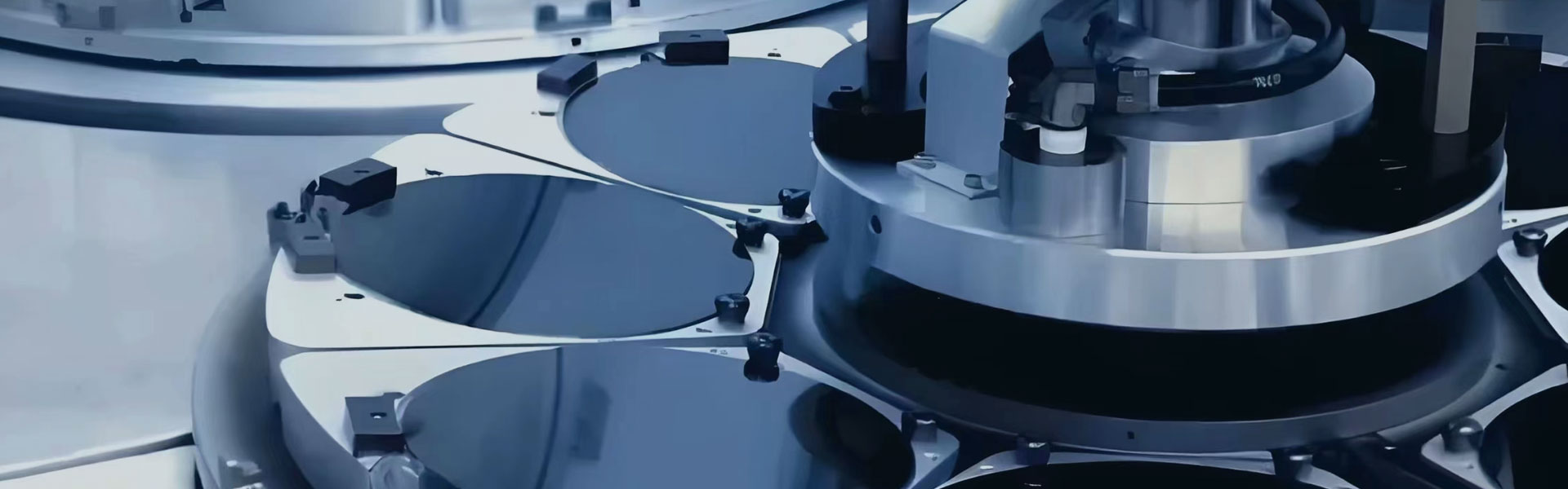


Physical Vapor Deposition
Vetek semiconductor Physical Vapor Deposition (PVD) is an advanced process technology widely used in surface treatment and thin film preparation. PVD technology uses physical methods to directly transform materials from solid or liquid to gas and form a thin film on the surface of the target substrate. This technology has the advantages of high precision, high uniformity and strong adhesion, and is widely used in semiconductors, optical devices, tool coatings and decorative coatings. Welcome to discuss with us!
Send Inquiry
Product Description
Vetek Semiconductor is a China manufacturer who supply advanced semiconductor materials in Physical Vapor Deposition Process like SiC coated crucible, glassy carbon crucible,SiC coating graphite heaters,Electron Beam Gun Evaporation Crucibles.
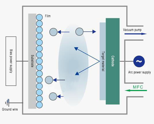
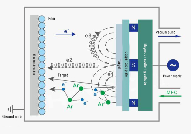
Basic principles of PVD process
Physical Vapor Deposition processes usually include a variety of specific methods such as evaporation, sputtering, and ion plating. Regardless of the method used, the basic principle of Physical Vapor Deposition is to vaporize the material from the source through high-temperature heating or ion bombardment. The vaporized material moves in the form of atoms or molecules in a vacuum or low-pressure environment and condenses into a thin film on the surface of the substrate. This process is mainly achieved by physical means, thus avoiding the influence of chemical reactions on the purity of the material.
Advantages of Physical Vapor Deposition technology
High purity and high density: PVD deposited films usually have high purity and density, which can significantly improve the performance of the coating, such as wear resistance, corrosion resistance and hardness.
Strong film adhesion: The PVD process can form a film with strong adhesion on the substrate, ensuring that the film is not easy to peel off during use, extending the service life of the product.
Wide range of material selection: PVD technology can be applied to a variety of materials, including metals, ceramics and alloys, and can prepare various functional coatings, such as conductive, insulating, heat-resistant and anti-oxidation coatings.
Environmental protection and sustainability: Compared with processes such as chemical vapor deposition (CVD), the Physical Vapor Deposition(PVD) process is more environmentally friendly, does not involve the generation of harmful gases, and reduces pollution to the environment.
Application of PVD technology
Semiconductor industry: In semiconductor manufacturing, Physical Vapor Deposition is often used in the preparation of thin film electrodes, diffusion barriers and metal interconnects to ensure that the components have good conductivity and stability.
Optical devices: Physical Vapor Deposition technology is widely used in optical coatings, such as anti-reflective coatings for mirrors and lenses, and the manufacture of optical filters to improve the performance of optical devices.
Hot Tags: Physical Vapor Deposition, China, Manufacturer, Supplier, Factory, Customized, Buy, Advanced, Durable, Made in China
Product Tag
Related Category
Tantalum Carbide Coating
Silicon Carbide Coating
Special Graphite
Carbon Fiber
Silicon Carbide Ceramics
Other Semiconductor Ceramics
Wafer
Surface Treatment Technology
Technical Service
Send Inquiry
Please feel free to give your inquiry in the form below. We will reply you in 24 hours.


