
- English
- Español
- Português
- русский
- Français
- 日本語
- Deutsch
- tiếng Việt
- Italiano
- Nederlands
- ภาษาไทย
- Polski
- 한국어
- Svenska
- magyar
- Malay
- বাংলা ভাষার
- Dansk
- Suomi
- हिन्दी
- Pilipino
- Türkçe
- Gaeilge
- العربية
- Indonesia
- Norsk
- تمل
- český
- ελληνικά
- український
- Javanese
- فارسی
- தமிழ்
- తెలుగు
- नेपाली
- Burmese
- български
- ລາວ
- Latine
- Қазақша
- Euskal
- Azərbaycan
- Slovenský jazyk
- Македонски
- Lietuvos
- Eesti Keel
- Română
- Slovenski
- मराठी
- Srpski језик
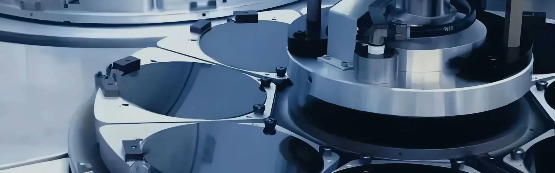


Porous SiC Vacuum Chuck
As a professional Porous SiC Vacuum Chuck manufacturer and supplier in China, Vetek Semiconductor's Porous SiC Vacuum Chuck is widely used in key components of semiconductor manufacturing equipment, especially when it comes to CVD and PECVD processes. Vetek Semiconductor specializes in manufacturing and supplying high-performance Porous SiC Vacuum Chuck. Welcome your further inquiries.
Send Inquiry
Product Description
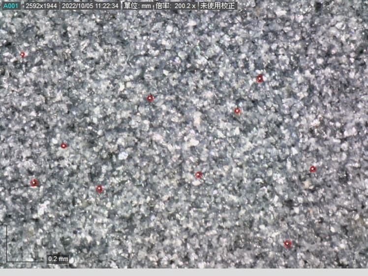
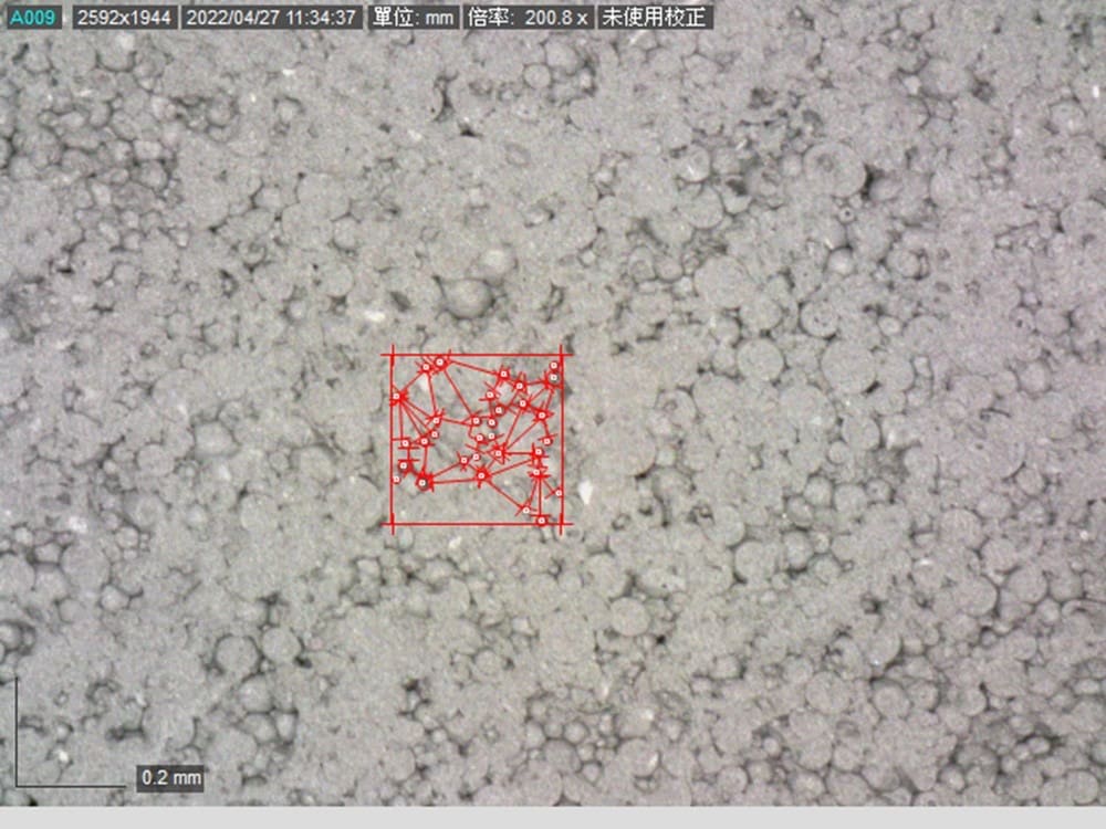
Vetek Semiconductor Porous SiC Vacuum Chuck is mainly composed of silicon carbide (SiC), a ceramic material with excellent performance. Porous SiC Vacuum Chuck can play the role of wafer support and fixation in the semiconductor processing process. This product can ensure the close fit between the wafer and the chuck by providing uniform suction, effectively avoiding the warping and deformation of the wafer, thereby ensuring the flatness of the flow during processing. In addition, the high temperature resistance of silicon carbide can ensure the stability of the chuck and prevent the wafer from falling off due to thermal expansion. Welcome to consult further.
In the field of electronics, Porous SiC Vacuum Chuck can be used as a semiconductor material for laser cutting, manufacturing power devices, photovoltaic modules and power electronic components. Its high thermal conductivity and high temperature resistance make it an ideal material for electronic devices. In the field of optoelectronics, Porous SiC Vacuum Chuck can be used to manufacture optoelectronic devices such as lasers, LED packaging materials and solar cells. Its excellent optical properties and corrosion resistance help improve the performance and stability of the device.
Vetek Semiconductor can provide:
1. Cleanliness: After SiC carrier processing, engraving, cleaning and final delivery, it must be tempered at 1200 degrees for 1.5 hours to burn out all impurities and then packed in vacuum bags.
2. Product flatness: Before placing the wafer, it must be above -60kpa when it is placed on the equipment to prevent the carrier from flying off during rapid transmission. After placing the wafer, it must be above -70kpa. If the no-load temperature is lower than -50kpa, the machine will keep alerting and cannot operate. Therefore, the flatness of the back is very important.
3. Gas path design: customized according to customer requirements.
3 stages of customer testing:
1. Oxidation test: no oxygen (the customer quickly heats up to 900 degrees, so the product needs to be annealed at 1100 degrees).
2. Metal residue test: Rapidly heat up to 1200 degrees, no metal impurities are released to contaminate the wafer.
3. Vacuum test: The difference between the pressure with and without Wafer is within +2ka (suction force).
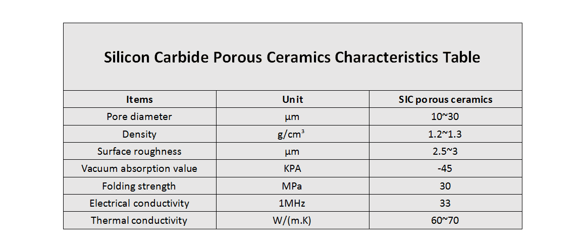
VeTek Semiconductor Porous SiC Vacuum Chuck Characteristics Table:
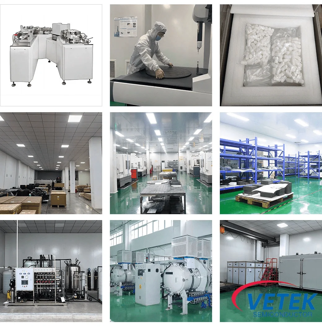
VeTek Semiconductor Porous SiC Vacuum Chuck shops:
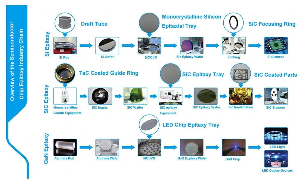
Overview of the semiconductor chip epitaxy industry chain:
Hot Tags: Porous SiC Vacuum Chuck, China, Manufacturer, Supplier, Factory, Customized, Buy, Advanced, Durable, Made in China
Product Tag
Related Category
Send Inquiry
Please feel free to give your inquiry in the form below. We will reply you in 24 hours.
Related Products


