
- English
- Español
- Português
- русский
- Français
- 日本語
- Deutsch
- tiếng Việt
- Italiano
- Nederlands
- ภาษาไทย
- Polski
- 한국어
- Svenska
- magyar
- Malay
- বাংলা ভাষার
- Dansk
- Suomi
- हिन्दी
- Pilipino
- Türkçe
- Gaeilge
- العربية
- Indonesia
- Norsk
- تمل
- český
- ελληνικά
- український
- Javanese
- فارسی
- தமிழ்
- తెలుగు
- नेपाली
- Burmese
- български
- ລາວ
- Latine
- Қазақша
- Euskal
- Azərbaycan
- Slovenský jazyk
- Македонски
- Lietuvos
- Eesti Keel
- Română
- Slovenski
- मराठी
- Srpski језик
Home
>
Products > Silicon Carbide Coating > ICP/PSS Etching Process > PSS Etching Carrier Plate for Semiconductor


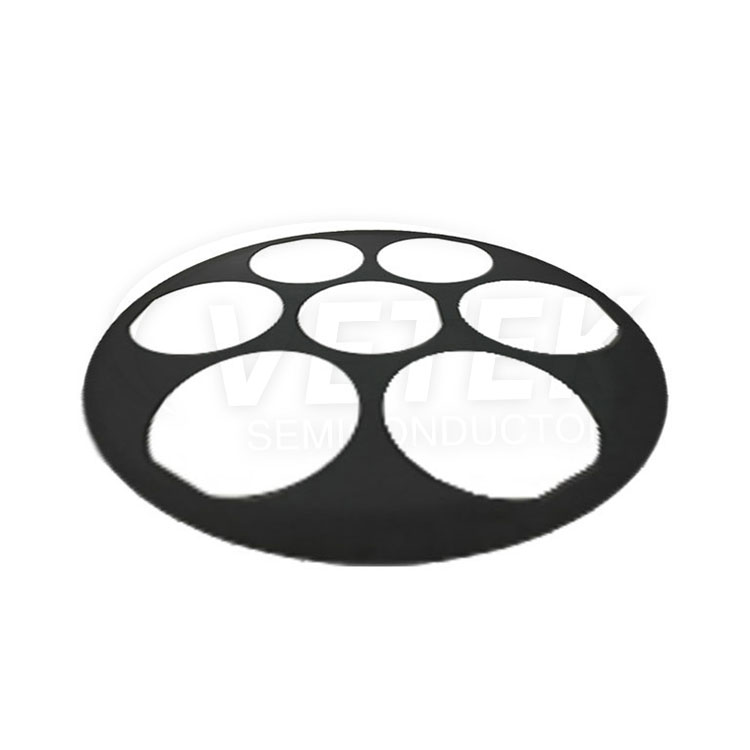
PSS Etching Carrier Plate for Semiconductor
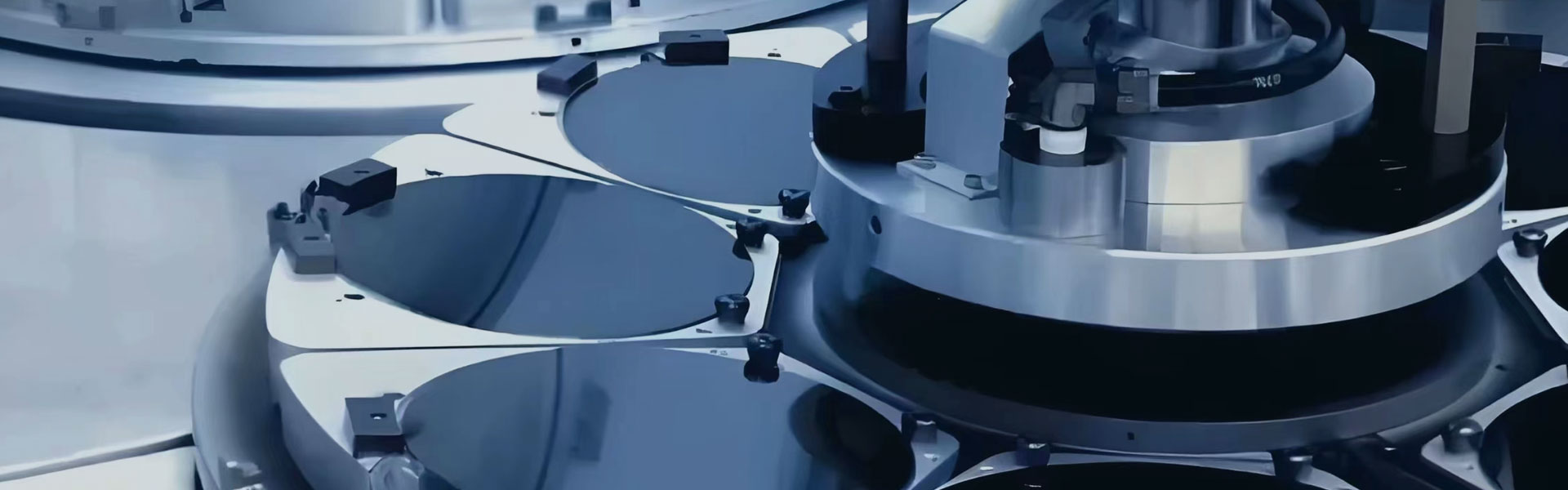
VeTek Semiconductor's PSS Etching Carrier Plate for Semiconductor is a high-quality, ultra-pure graphite carrier designed for wafer handling processes. Our carriers have excellent performance and can perform well in harsh environments, high temperatures and harsh chemical cleaning conditions. Our products are widely used in many European and American markets, and we look forward to becoming your long-term partner in China.
Send Inquiry
Product Description
As the professional manufacturer, we would like to provide you high quality PSS Etching Carrier Plate for Semiconductor. VeTek Semiconductor's PSS Etching Carrier Plate for Semiconductor is a specialized component used in the semiconductor industry for the process of Plasma Source Spectroscopy (PSS) etching. This plate plays a crucial role in supporting and carrying the semiconductor wafers during the etching process.Welcome to inquiry us!
PSS Etching Carrier Plate for Semiconductor Key Features:
● Precision Design: The carrier plate is engineered with precise dimensions and surface flatness to ensure uniform and consistent etching across the semiconductor wafers. It provides a stable and controlled platform for the wafers, allowing for accurate and reliable etching results.
● Plasma Resistance: The carrier plate exhibits excellent resistance to the plasma used in the etching process. It remains unaffected by the reactive gases and high-energy plasma, ensuring prolonged service life and consistent performance.
● Thermal Conductivity: The carrier plate features high thermal conductivity to efficiently dissipate heat generated during the etching process. This helps in maintaining optimal temperature control and prevents overheating of the semiconductor wafers.
● Compatibility: The PSS Etching Carrier Plate is designed to be compatible with various semiconductor wafer sizes commonly used in the industry, ensuring versatility and ease of use across different manufacturing processes.
Product parameter of the PSS Etching Carrier Plate for Semiconductor
| Basic physical properties of CVD SiC coating | |
| Property | Typical Value |
| Crystal Structure | FCC β phase polycrystalline, mainly (111) oriented |
| SiC coating Density | 3.21 g/cm³ |
| CVD SiC coating Hardness | 2500 Vickers hardness(500g load) |
| Grain Size | 2~10μm |
| Chemical Purity | 99.99995% |
| Heat Capacity | 640 J·kg-1·K-1 |
| Sublimation Temperature | 2700℃ |
| Flexural Strength | 415 MPa RT 4-point |
| Young's Modulus | 430 Gpa 4pt bend, 1300℃ |
| Thermal Conductivity | 300W·m-1·K-1 |
| Thermal Expansion(CTE) | 4.5×10⁻⁶K-1 |
VeTek Semiconductor PSS Etching Carrier Plate for Semiconductor Production Shop


Overview of the semiconductor chip epitaxy industry chain:

Hot Tags: PSS Etching Carrier Plate for Semiconductor, China, Manufacturer, Supplier, Factory, Customized, Buy, Advanced, Durable, Made in China
Product Tag
Related Category
Solid Silicon Carbide
Silicon Epitaxy
Silicon Carbide Epitaxy
MOCVD Technology
RTA/RTP Process
ICP/PSS Etching Process
Other Process
ALD
Send Inquiry
Please feel free to give your inquiry in the form below. We will reply you in 24 hours.


