
- English
- Español
- Português
- русский
- Français
- 日本語
- Deutsch
- tiếng Việt
- Italiano
- Nederlands
- ภาษาไทย
- Polski
- 한국어
- Svenska
- magyar
- Malay
- বাংলা ভাষার
- Dansk
- Suomi
- हिन्दी
- Pilipino
- Türkçe
- Gaeilge
- العربية
- Indonesia
- Norsk
- تمل
- český
- ελληνικά
- український
- Javanese
- فارسی
- தமிழ்
- తెలుగు
- नेपाली
- Burmese
- български
- ລາວ
- Latine
- Қазақша
- Euskal
- Azərbaycan
- Slovenský jazyk
- Македонски
- Lietuvos
- Eesti Keel
- Română
- Slovenski
- मराठी
- Srpski језик

8-inch SiC epitaxial furnace and homoepitaxial process research
2024-08-29
Currently, the SiC industry is transforming from 150 mm (6 inches) to 200 mm (8 inches). In order to meet the urgent demand for large-size, high-quality SiC homoepitaxial wafers in the industry, 150 mm and 200 mm 4H-SiC homoepitaxial wafers were successfully prepared on domestic substrates using the independently developed 200 mm SiC epitaxial growth equipment. A homoepitaxial process suitable for 150 mm and 200 mm was developed, in which the epitaxial growth rate can be greater than 60 μm/h. While meeting the high-speed epitaxy, the epitaxial wafer quality is excellent. The thickness uniformity of 150 mm and 200 mm SiC epitaxial wafers can be controlled within 1.5%, the concentration uniformity is less than 3%, the fatal defect density is less than 0.3 particles/cm2, and the epitaxial surface roughness root mean square Ra is less than 0.15 nm, and all core process indicators are at the advanced level of the industry.
Silicon Carbide (SiC) is one of the representatives of the third-generation semiconductor materials. It has the characteristics of high breakdown field strength, excellent thermal conductivity, large electron saturation drift velocity, and strong radiation resistance. It has greatly expanded the energy processing capacity of power devices and can meet the service requirements of the next generation of power electronic equipment for devices with high power, small size, high temperature, high radiation and other extreme conditions. It can reduce space, reduce power consumption and reduce cooling requirements. It has brought revolutionary changes to new energy vehicles, rail transportation, smart grids and other fields. Therefore, silicon carbide semiconductors have become recognized as the ideal material that will lead the next generation of high-power power electronic devices. In recent years, thanks to the national policy support for the development of the third-generation semiconductor industry, the research and development and construction of the 150 mm SiC device industry system have been basically completed in China, and the security of the industrial chain has been basically guaranteed. Therefore, the focus of the industry has gradually shifted to cost control and efficiency improvement. As shown in Table 1, compared with 150 mm, 200 mm SiC has a higher edge utilization rate, and the output of single wafer chips can be increased by about 1.8 times. After the technology matures, the manufacturing cost of a single chip can be reduced by 30%. The technological breakthrough of 200 mm is a direct means of "reducing costs and increasing efficiency", and it is also the key for my country's semiconductor industry to "run parallel" or even "lead".
Different from the Si device process, SiC semiconductor power devices are all processed and prepared with epitaxial layers as the cornerstone. Epitaxial wafers are essential basic materials for SiC power devices. The quality of the epitaxial layer directly determines the yield of the device, and its cost accounts for 20% of the chip manufacturing cost. Therefore, epitaxial growth is an essential intermediate link in SiC power devices. The upper limit of epitaxial process level is determined by epitaxial equipment. At present, the localization degree of domestic 150 mm SiC epitaxial equipment is relatively high, but the overall layout of 200 mm lags behind the international level at the same time. Therefore, in order to solve the urgent needs and bottleneck problems of large-size, high-quality epitaxial material manufacturing for the development of the domestic third-generation semiconductor industry, this paper introduces the 200 mm SiC epitaxial equipment successfully developed in my country, and studies the epitaxial process. By optimizing the process parameters such as process temperature, carrier gas flow rate, C/Si ratio, etc., the concentration uniformity <3%, thickness non-uniformity <1.5%, roughness Ra <0.2 nm and fatal defect density <0.3 particles/cm2 of 150 mm and 200 mm SiC epitaxial wafers with self-developed 200 mm silicon carbide epitaxial furnace are obtained. The equipment process level can meet the needs of high-quality SiC power device preparation.
1 Experiments
1.1 Principle of SiC epitaxial process
The 4H-SiC homoepitaxial growth process mainly includes 2 key steps, namely, high-temperature in-situ etching of 4H-SiC substrate and homogeneous chemical vapor deposition process. The main purpose of substrate in-situ etching is to remove the subsurface damage of the substrate after wafer polishing, residual polishing liquid, particles and oxide layer, and a regular atomic step structure can be formed on the substrate surface by etching. In-situ etching is usually carried out in a hydrogen atmosphere. According to the actual process requirements, a small amount of auxiliary gas can also be added, such as hydrogen chloride, propane, ethylene or silane. The temperature of in-situ hydrogen etching is generally above 1 600 ℃, and the pressure of the reaction chamber is generally controlled below 2×10⁴ Pa during the etching process.
After the substrate surface is activated by in-situ etching, it enters the high-temperature chemical vapor deposition process, that is, the growth source (such as ethylene/propane, TCS/silane), doping source (n-type doping source nitrogen, p-type doping source TMAl), and auxiliary gas such as hydrogen chloride are transported to the reaction chamber through a large flow of carrier gas (usually hydrogen). After the gas reacts in the high-temperature reaction chamber, part of the precursor reacts chemically and adsorbs on the wafer surface, and a single-crystal homogeneous 4H-SiC epitaxial layer with a specific doping concentration, specific thickness, and higher quality is formed on the substrate surface using the single-crystal 4H-SiC substrate as a template. After years of technical exploration, the 4H-SiC homoepitaxial technology has basically matured and is widely used in industrial production. The most widely used 4H-SiC homoepitaxial technology in the world has two typical characteristics: (1) Using an off-axis (relative to the <0001> crystal plane, toward the <11-20> crystal direction) oblique cut substrate as a template, a high-purity single-crystal 4H-SiC epitaxial layer without impurities is deposited on the substrate in the form of step-flow growth mode. Early 4H-SiC homoepitaxial growth used a positive crystal substrate, that is, the <0001> Si plane for growth. The density of atomic steps on the surface of the positive crystal substrate is low and the terraces are wide. Two-dimensional nucleation growth is easy to occur during the epitaxy process to form 3C crystal SiC (3C-SiC). By off-axis cutting, high-density, narrow terrace width atomic steps can be introduced on the surface of the 4H-SiC <0001> substrate, and the adsorbed precursor can effectively reach the atomic step position with relatively low surface energy through surface diffusion. At the step, the precursor atom/molecular group bonding position is unique, so in the step flow growth mode, the epitaxial layer can perfectly inherit the Si-C double atomic layer stacking sequence of the substrate to form a single crystal with the same crystal phase as the substrate. (2) High-speed epitaxial growth is achieved by introducing a chlorine-containing silicon source. In conventional SiC chemical vapor deposition systems, silane and propane (or ethylene) are the main growth sources. In the process of increasing the growth rate by increasing the growth source flow rate, as the equilibrium partial pressure of the silicon component continues to increase, it is easy to form silicon clusters by homogeneous gas phase nucleation, which significantly reduces the utilization rate of the silicon source. The formation of silicon clusters greatly limits the improvement of the epitaxial growth rate. At the same time, silicon clusters can disturb the step flow growth and cause defect nucleation. In order to avoid homogeneous gas phase nucleation and increase the epitaxial growth rate, the introduction of chlorine-based silicon sources is currently the mainstream method to increase the epitaxial growth rate of 4H-SiC.
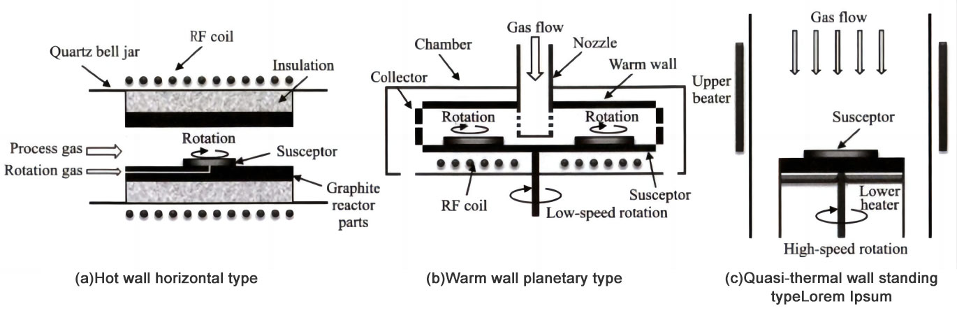
1.2 200 mm (8-inch) SiC epitaxial equipment and process conditions
The experiments described in this paper were all conducted on a 150/200 mm (6/8-inch) compatible monolithic horizontal hot wall SiC epitaxial equipment independently developed by the 48th Institute of China Electronics Technology Group Corporation. The epitaxial furnace supports fully automatic wafer loading and unloading. Figure 1 is a schematic diagram of the internal structure of the reaction chamber of the epitaxial equipment. As shown in Figure 1, the outer wall of the reaction chamber is a quartz bell with a water-cooled interlayer, and the inside of the bell is a high-temperature reaction chamber, which is composed of thermal insulation carbon felt, high-purity special graphite cavity, graphite gas-floating rotating base, etc. The entire quartz bell is covered with a cylindrical induction coil, and the reaction chamber inside the bell is electromagnetically heated by a medium-frequency induction power supply. As shown in Figure 1 (b), the carrier gas, reaction gas, and doping gas all flow through the wafer surface in a horizontal laminar flow from the upstream of the reaction chamber to the downstream of the reaction chamber and are discharged from the tail gas end. To ensure the consistency within the wafer, the wafer carried by the air floating base is always rotated during the process.
The substrate used in the experiment is a commercial 150 mm, 200 mm (6 inches, 8 inches) <1120> direction 4° off-angle conductive n-type 4H-SiC double-sided polished SiC substrate produced by Shanxi Shuoke Crystal. Trichlorosilane (SiHCl3, TCS) and ethylene (C2H4) are used as the main growth sources in the process experiment, among which TCS and C2H4 are used as silicon source and carbon source respectively, high-purity nitrogen (N2) is used as n-type doping source, and hydrogen (H2) is used as dilution gas and carrier gas. The epitaxial process temperature range is 1 600 ~1 660 ℃, the process pressure is 8×10³ ~12×103 Pa, and the H2 carrier gas flow rate is 100~140 L/min.
1.3 Epitaxial wafer testing and characterization
Fourier infrared spectrometer (equipment manufacturer Thermalfisher, model iS50) and mercury probe concentration tester (equipment manufacturer Semilab, model 530L) were used to characterize the mean and distribution of epitaxial layer thickness and doping concentration; the thickness and doping concentration of each point in the epitaxial layer were determined by taking points along the diameter line intersecting the normal line of the main reference edge at 45° at the center of the wafer with 5 mm edge removal. For a 150 mm wafer, 9 points were taken along a single diameter line (two diameters were perpendicular to each other), and for a 200 mm wafer, 21 points were taken, as shown in Figure 2. An atomic force microscope (equipment manufacturer Bruker, model Dimension Icon) was used to select 30 μm×30 μm areas in the center area and the edge area (5 mm edge removal) of the epitaxial wafer to test the surface roughness of the epitaxial layer; the defects of the epitaxial layer were measured using a surface defect tester (equipment manufacturer China Electronics Kefenghua, model Mars 4410 pro) for characterization.
2 Experimental results and discussion
2.1 Epitaxial layer thickness and uniformity
Epitaxial layer thickness, doping concentration and uniformity are one of the core indicators for judging the quality of epitaxial wafers. Accurately controllable thickness, doping concentration and uniformity within the wafer are the key to ensuring the performance and consistency of SiC power devices, and epitaxial layer thickness and doping concentration uniformity are also important bases for measuring the process capability of epitaxial equipment.
Figure 3 shows the thickness uniformity and distribution curve of 150 mm and 200 mm SiC epitaxial wafers. It can be seen from the figure that the epitaxial layer thickness distribution curve is symmetrical about the center point of the wafer. The epitaxial process time is 600 s, the average epitaxial layer thickness of the 150 mm epitaxial wafer is 10.89 μm, and the thickness uniformity is 1.05%. By calculation, the epitaxial growth rate is 65.3 μm/h, which is a typical fast epitaxial process level. Under the same epitaxial process time, the epitaxial layer thickness of the 200 mm epitaxial wafer is 10.10 μm, the thickness uniformity is within 1.36%, and the overall growth rate is 60.60 μm/h, which is slightly lower than the 150 mm epitaxial growth rate. This is because there is obvious loss along the way when the silicon source and carbon source flow from the upstream of the reaction chamber through the wafer surface to the downstream of the reaction chamber, and the 200 mm wafer area is larger than the 150 mm. The gas flows through the surface of the 200 mm wafer for a longer distance, and the source gas consumed along the way is more. Under the condition that the wafer keeps rotating, the overall thickness of the epitaxial layer is thinner, so the growth rate is slower. Overall, the thickness uniformity of 150 mm and 200 mm epitaxial wafers is excellent, and the process capability of the equipment can meet the requirements of high-quality devices.
2.2 Epitaxial layer doping concentration and uniformity
Figure 4 shows the doping concentration uniformity and curve distribution of 150 mm and 200 mm SiC epitaxial wafers. As can be seen from the figure, the concentration distribution curve on the epitaxial wafer has obvious symmetry relative to the center of the wafer. The doping concentration uniformity of the 150 mm and 200 mm epitaxial layers is 2.80% and 2.66% respectively, which can be controlled within 3%, which is an excellent level among international similar equipment. The doping concentration curve of the epitaxial layer is distributed in a "W" shape along the diameter direction, which is mainly determined by the flow field of the horizontal hot wall epitaxial furnace, because the airflow direction of the horizontal airflow epitaxial growth furnace is from the air inlet end (upstream) and flows out from the downstream end in a laminar flow through the wafer surface; because the "along-the-way depletion" rate of the carbon source (C2H4) is higher than that of the silicon source (TCS), when the wafer rotates, the actual C/Si on the wafer surface gradually decreases from the edge to the center (the carbon source in the center is less), according to the "competitive position theory" of C and N, the doping concentration in the center of the wafer gradually decreases toward the edge. In order to obtain excellent concentration uniformity, the edge N2 is added as compensation during the epitaxial process to slow down the decrease in doping concentration from the center to the edge, so that the final doping concentration curve presents a "W" shape.
2.3 Epitaxial layer defects
In addition to thickness and doping concentration, the level of epitaxial layer defect control is also a core parameter for measuring the quality of epitaxial wafers and an important indicator of the process capability of epitaxial equipment. Although SBD and MOSFET have different requirements for defects, more obvious surface morphology defects such as drop defects, triangle defects, carrot defects, and comet defects are defined as killer defects for SBD and MOSFET devices. The probability of failure of chips containing these defects is high, so controlling the number of killer defects is extremely important for improving chip yield and reducing costs. Figure 5 shows the distribution of killer defects of 150 mm and 200 mm SiC epitaxial wafers. Under the condition that there is no obvious imbalance in the C/Si ratio, carrot defects and comet defects can be basically eliminated, while drop defects and triangle defects are related to the cleanliness control during the operation of epitaxial equipment, the impurity level of graphite parts in the reaction chamber, and the quality of the substrate. From Table 2, we can see that the fatal defect density of 150 mm and 200 mm epitaxial wafers can be controlled within 0.3 particles/cm2, which is an excellent level for the same type of equipment. The fatal defect density control level of 150 mm epitaxial wafer is better than that of 200 mm epitaxial wafer. This is because the 150 mm substrate preparation process is more mature than that of 200 mm, the substrate quality is better, and the impurity control level of 150 mm graphite reaction chamber is better.
2.4 Epitaxial wafer surface roughness
Figure 6 shows the AFM images of the surface of 150 mm and 200 mm SiC epitaxial wafers. As can be seen from the figure, the surface root mean square roughness Ra of 150 mm and 200 mm epitaxial wafers is 0.129 nm and 0.113 nm respectively, and the surface of the epitaxial layer is smooth, without obvious macro-step aggregation phenomenon, which indicates that the growth of the epitaxial layer always maintains the step flow growth mode during the entire epitaxial process, and no step aggregation occurs. It can be seen that the epitaxial layer with a smooth surface can be obtained on 150 mm and 200 mm low-angle substrates by using the optimized epitaxial growth process.
3. Conclusions
150 mm and 200 mm 4H-SiC homoepitaxial wafers were successfully prepared on domestic substrates using the self-developed 200 mm SiC epitaxial growth equipment, and a homoepitaxial process suitable for 150 mm and 200 mm was developed. The epitaxial growth rate can be greater than 60 μm/h. While meeting the high-speed epitaxy requirement, the epitaxial wafer quality is excellent. The thickness uniformity of 150 mm and 200 mm SiC epitaxial wafers can be controlled within 1.5%, the concentration uniformity is less than 3%, the fatal defect density is less than 0.3 particles/cm2, and the epitaxial surface roughness root mean square Ra is less than 0.15 nm. The core process indicators of the epitaxial wafers are at the advanced level in the industry.
------------------------------------------------------------------------------------------------------------------------------------------------------------------------------------------------------------------------------------------------------------------------------------------
VeTek Semiconductor is a professional Chinese manufacturer of CVD SiC Coated Ceiling, CVD SiC Coating Nozzle, and SiC Coating Inlet Ring. VeTek Semiconductor is committed to providing advanced solutions for various SiC Wafer products for the semiconductor industry.
If you are interested in 8-inch SiC epitaxial furnace and homoepitaxial process, please feel free to contact us directly.
Mob: +86-180 6922 0752
WhatsAPP: +86 180 6922 0752
Email: anny@veteksemi.com


