
- English
- Español
- Português
- русский
- Français
- 日本語
- Deutsch
- tiếng Việt
- Italiano
- Nederlands
- ภาษาไทย
- Polski
- 한국어
- Svenska
- magyar
- Malay
- বাংলা ভাষার
- Dansk
- Suomi
- हिन्दी
- Pilipino
- Türkçe
- Gaeilge
- العربية
- Indonesia
- Norsk
- تمل
- český
- ελληνικά
- український
- Javanese
- فارسی
- தமிழ்
- తెలుగు
- नेपाली
- Burmese
- български
- ລາວ
- Latine
- Қазақша
- Euskal
- Azərbaycan
- Slovenský jazyk
- Македонски
- Lietuvos
- Eesti Keel
- Română
- Slovenski
- मराठी
- Srpski језик

Semiconductor substrate wafer: Material properties of silicon, GaAs, SiC and GaN
2024-08-28
01. Basics of semiconductor substrate wafer
1.1 Definition of semiconductor substrate
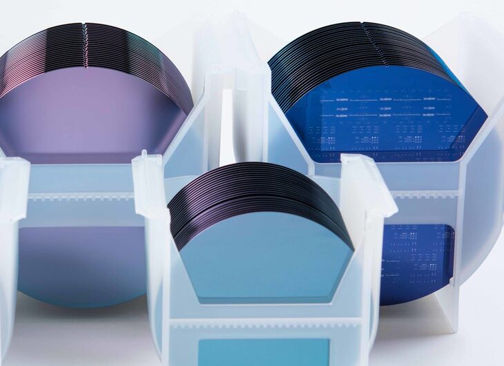
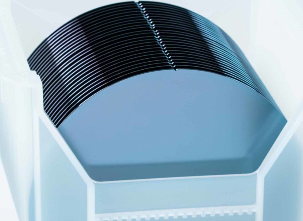
Semiconductor substrate refers to the basic material used in the manufacture of semiconductor devices, usually single crystal or polycrystalline materials made by highly purified and crystal growth technology. Substrate wafers are usually thin and solid sheet structures, on which various semiconductor devices and circuits are manufactured. The purity and quality of the substrate directly affect the performance and reliability of the final semiconductor device.
1.2 The role and application field of substrate wafers
Substrate wafers play a vital role in the semiconductor manufacturing process. As the basis of devices and circuits, substrate wafers not only support the structure of the entire device, but also provide necessary support in electrical, thermal and mechanical aspects. Its main functions include:
Mechanical support: Provide a stable structural foundation to support subsequent manufacturing steps.
Thermal management: Help dissipate heat to prevent overheating from affecting device performance.
Electrical characteristics: Affect the electrical properties of the device, such as conductivity, carrier mobility, etc.
In terms of application fields, substrate wafers are widely used in:
Microelectronic devices: such as integrated circuits (ICs), microprocessors, etc.
Optoelectronic devices: such as LEDs, lasers, photodetectors, etc.
High-frequency electronic devices: such as RF amplifiers, microwave devices, etc.
Power electronic devices: such as power converters, inverters, etc.
02. Semiconductor materials and their properties
Silicon (Si) substrate
· The difference between single crystal silicon and polycrystalline silicon:
Silicon is the most commonly used semiconductor material, mainly in the form of single crystal silicon and polycrystalline silicon. Single crystal silicon is composed of a continuous crystal structure, with high purity and defect-free characteristics, which is very suitable for high-performance electronic devices. Polycrystalline silicon is composed of multiple grains, and there are grain boundaries between the grains. Although the manufacturing cost is low, the electrical performance is poor, so it is usually used in some low-performance or large-scale application scenarios, such as solar cells.
· Electronic properties and advantages of silicon substrate:
Silicon substrate has good electronic properties, such as high carrier mobility and moderate energy gap (1.1 eV), which make silicon an ideal material for manufacturing most semiconductor devices.
In addition, silicon substrates have the following advantages:
High purity: Through advanced purification and growth techniques, very high purity single crystal silicon can be obtained.
Cost-effectiveness: Compared with other semiconductor materials, silicon has a low cost and a mature manufacturing process.
Oxide formation: Silicon can naturally form a layer of silicon dioxide (SiO2), which can serve as a good insulating layer in device manufacturing.
Gallium arsenide (GaAs) substrate
· High-frequency characteristics of GaAs:
Gallium arsenide is a compound semiconductor that is particularly suitable for high-frequency and high-speed electronic devices due to its high electron mobility and wide bandgap. GaAs devices can operate at higher frequencies with higher efficiency and lower noise levels. This makes GaAs an important material in microwave and millimeter wave applications.
· Application of GaAs in optoelectronics and high-frequency electronic devices:
Due to its direct bandgap, GaAs is also widely used in optoelectronic devices. For example, GaAs materials are widely used in the manufacture of LEDs and lasers. In addition, the high electron mobility of GaAs makes it perform well in RF amplifiers, microwave devices, and satellite communication equipment.
Silicon Carbide (SiC) Substrate
· Thermal conductivity and high power properties of SiC:
Silicon carbide is a wide bandgap semiconductor with excellent thermal conductivity and high breakdown electric field. These properties make SiC very suitable for high power and high temperature applications. SiC devices can operate stably at voltages and temperatures several times higher than silicon devices.
· Advantages of SiC in power electronic devices:
SiC substrates show significant advantages in power electronic devices, such as lower switching losses and higher efficiency. This makes SiC increasingly popular in high power conversion applications such as electric vehicles, wind and solar inverters. In addition, SiC is widely used in aerospace and industrial control due to its high temperature resistance.
Gallium Nitride (GaN) Substrate
· High electron mobility and optical properties of GaN:
Gallium nitride is another wide bandgap semiconductor with extremely high electron mobility and strong optical properties. The high electron mobility of GaN makes it very efficient in high frequency and high power applications. At the same time, GaN can emit light in the ultraviolet to visible range, suitable for a variety of optoelectronic devices.
· Application of GaN in power and optoelectronic devices:
In the field of power electronics, GaN devices excel in switching power supplies and RF amplifiers due to their high breakdown electric field and low on-resistance. At the same time, GaN also plays an important role in optoelectronic devices, especially in the manufacture of LEDs and laser diodes, promoting the advancement of lighting and display technologies.
· Potential of emerging materials in semiconductors:
With the development of science and technology, emerging semiconductor materials such as gallium oxide (Ga2O3) and diamond have shown great potential. Gallium oxide has an ultra-wide bandgap (4.9 eV) and is very suitable for high-power electronic devices, while diamond is considered to be an ideal material for the next generation of high-power and high-frequency applications due to its excellent thermal conductivity and extremely high carrier mobility. These new materials are expected to play an important role in future electronic and optoelectronic devices.
03. Wafer manufacturing process
3.1 Growth technology of substrate wafers
3.1.1 Czochralski method (CZ method)
The Czochralski method is the most commonly used method for manufacturing single-crystal silicon wafers. It is done by immersing a seed crystal into molten silicon and then slowly pulling it out, so that the molten silicon crystallizes on the seed crystal and grows into a single crystal. This method can produce large-sized, high-quality single-crystal silicon, which is very suitable for the manufacture of large-scale integrated circuits.
3.1.2 Bridgman method
The Bridgman method is commonly used to grow compound semiconductors, such as gallium arsenide. In this method, the raw materials are heated to a molten state in a crucible and then slowly cooled to form a single crystal. The Bridgman method can control the growth rate and direction of the crystal and is suitable for the production of complex compound semiconductors.
3.1.3 Molecular beam epitaxy (MBE)
Molecular beam epitaxy is a technology used to grow ultra-thin semiconductor layers on substrates. It forms high-quality crystal layers by precisely controlling molecular beams of different elements in an ultra-high vacuum environment and depositing them layer by layer on the substrate. MBE technology is particularly suitable for the manufacture of high-precision quantum dots and ultra-thin heterojunction structures.
3.1.4 Chemical vapor deposition (CVD)
Chemical vapor deposition is a thin film deposition technology widely used in the manufacture of semiconductors and other high-performance materials. CVD decomposes gaseous precursors and deposits them on the substrate surface to form a solid film. CVD technology can produce films with highly controlled thickness and composition, which is very suitable for the manufacture of complex devices.
3.2 Wafer cutting and polishing
3.2.1 Silicon wafer cutting technology
After the crystal growth is completed, the large crystal will be cut into thin slices to become wafers. Silicon wafer cutting usually uses diamond saw blades or wire saw technology to ensure the cutting accuracy and reduce material loss. The cutting process needs to be precisely controlled to ensure that the thickness and surface flatness of the wafer meet the requirements.
---------------------------------------------------------------------------------------------------------------------------------------------------------------------------------------------------------------------------------------------------------------------------------------------------
VeTek Semiconductor is a professional Chinese manufacturer of 4°off axis p-type SiC Wafer, 4H N type SiC Substrate, and 4H Semi Insulating type SiC Substrate. VeTek Semiconductor is committed to providing advanced solutions for various SiC Wafer products for the semiconductor industry.
If you are interested in Semiconductor substrate wafers, please feel free to contact us directly.
Mob: +86-180 6922 0752
WhatsAPP: +86 180 6922 0752
Email: anny@veteksemi.com


