
- English
- Español
- Português
- русский
- Français
- 日本語
- Deutsch
- tiếng Việt
- Italiano
- Nederlands
- ภาษาไทย
- Polski
- 한국어
- Svenska
- magyar
- Malay
- বাংলা ভাষার
- Dansk
- Suomi
- हिन्दी
- Pilipino
- Türkçe
- Gaeilge
- العربية
- Indonesia
- Norsk
- تمل
- český
- ελληνικά
- український
- Javanese
- فارسی
- தமிழ்
- తెలుగు
- नेपाली
- Burmese
- български
- ລາວ
- Latine
- Қазақша
- Euskal
- Azərbaycan
- Slovenský jazyk
- Македонски
- Lietuvos
- Eesti Keel
- Română
- Slovenski
- मराठी
- Srpski језик

How thin can the Taiko process make silicon wafers?
2024-09-04
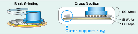
What is the Taiko process?
The Taiko process is a wafer thinning technology that leaves the edge of the wafer unthinned and only thins the central area of the wafer. This allows the central area of the wafer to reach an extremely thin thickness, while the edge of the wafer maintains its original thickness.
Why use the Taiko process?
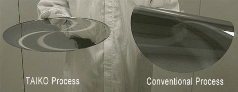
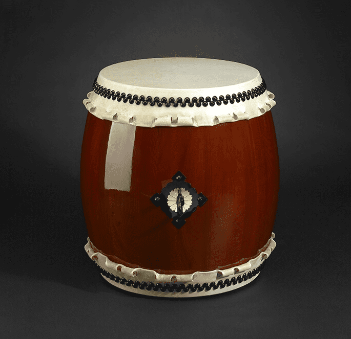
As shown in the figure above, the traditional thinning process thins the entire wafer, causing the overall structure of the wafer to become very fragile, extremely fragile during the production process, and excessive warping, which is not conducive to subsequent manufacturing. The Taiko process gives the entire wafer higher mechanical strength, which perfectly solves this problem. Why is it called the Taiko process? The Taiko process is a process invented by the Japanese Disco company. The inspiration for its name comes from the Japanese Taiko drum (Taiko drum), which has thick edges and thinner middle parts, hence the name.
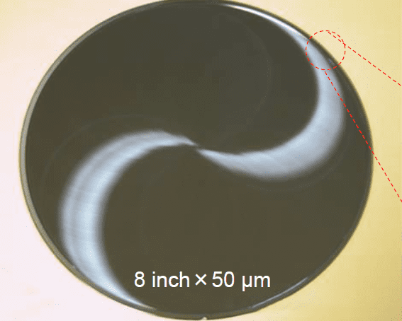
What is the minimum thickness that the Taiko process can thin to?
The above picture shows the effect of an 8-inch wafer with a thickness of 50um. The second picture in this article shows the effect of a 12-inch wafer thinned to 50um.
--------------------------------------------------------------------------------------------------------------------------------------------------------------------------------------------------------------------------------------------------------------------------------------------------------------------
VeTek Semiconductor is a professional Chinese manufacturer of SiC Wafer,Wafer Carrier,Wafer Boat,Wafer Chuck. VeTek Semiconductor is committed to providing advanced solutions for various SiC Wafer products for the semiconductor industry.
If you are interested in our wafer products, please do not hesitate to contact us.We sincerely look forward to your further consultation.
Mob: +86-180 6922 0752
WhatsAPP: +86 180 6922 0752
Email: anny@veteksemi.com
Previous:How much do you know about sapphire?


