
- English
- Español
- Português
- русский
- Français
- 日本語
- Deutsch
- tiếng Việt
- Italiano
- Nederlands
- ภาษาไทย
- Polski
- 한국어
- Svenska
- magyar
- Malay
- বাংলা ভাষার
- Dansk
- Suomi
- हिन्दी
- Pilipino
- Türkçe
- Gaeilge
- العربية
- Indonesia
- Norsk
- تمل
- český
- ελληνικά
- український
- Javanese
- فارسی
- தமிழ்
- తెలుగు
- नेपाली
- Burmese
- български
- ລາວ
- Latine
- Қазақша
- Euskal
- Azərbaycan
- Slovenský jazyk
- Македонски
- Lietuvos
- Eesti Keel
- Română
- Slovenski
- मराठी
- Srpski језик

The Development History of 3C SiC
2024-07-29
As an important form of silicon carbide, the development history of 3C-SiC reflects the continuous progress of semiconductor material science. In the 1980s, Nishino et al. first obtained 4um 3C-SiC thin films on silicon substrates by chemical vapor deposition (CVD) [1], which laid the foundation for 3C-SiC thin film technology.
The 1990s was the golden age of SiC research. Cree Research Inc. launched 6H-SiC and 4H-SiC chips in 1991 and 1994 respectively, promoting the commercialization of SiC semiconductor devices. The technological progress during this period laid the foundation for the subsequent research and application of 3C-SiC.
In the early 21st century, domestic silicon-based SiC thin films also developed to a certain extent. Ye Zhizhen et al. prepared silicon-based SiC thin films by CVD under low temperature conditions in 2002 [2]. In 2001, An Xia et al. prepared silicon-based SiC thin films by magnetron sputtering at room temperature [3].
However, due to the large difference between the lattice constant of Si and that of SiC (about 20%), the defect density of 3C-SiC epitaxial layer is relatively high, especially the twin defect such as DPB. In order to reduce the lattice mismatch, researchers use 6H-SiC, 15R-SiC or 4H-SiC on the (0001) surface as substrate to grow 3C-SiC epitaxial layer and reduce the defect density. For example, in 2012, Seki, Kazuaki et al. proposed the dynamic polymorphic epitaxy control technology, which realizes the polymorphic selective growth of 3C-SiC and 6H-SiC on the 6H-SiC (0001) surface seed by controlling the supersaturation [4-5]. In 2023, researchers such as Xun Li used the CVD method to optimize the growth and process, and successfully obtained a smooth 3C-SiC epitaxial layer with no DPB defects on the surface on a 4H-SiC substrate at a growth rate of 14um/h[6].
Crystal Structure and Application Fields of 3C SiC
Among many SiCD polytypes, 3C-SiC is the only cubic polytype, also known as β-SiC. In this crystal structure, Si and C atoms exist in a one-to-one ratio in the lattice, and each atom is surrounded by four heterogeneous atoms, forming a tetrahedral structural unit with strong covalent bonds. The structural feature of 3C-SiC is that the Si-C diatomic layers are repeatedly arranged in the order of ABC-ABC-…, and each unit cell contains three such diatomic layers, which is called C3 representation; the crystal structure of 3C-SiC is shown in the figure below:
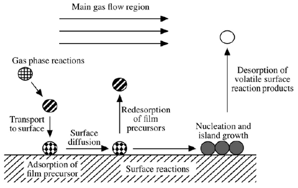
Figure 1 Crystal structure of 3C-SiC
Currently, silicon (Si) is the most commonly used semiconductor material for power devices. However, due to the performance of Si, silicon-based power devices are limited. Compared with 4H-SiC and 6H-SiC, 3C-SiC has the highest room temperature theoretical electron mobility (1000 cm·V-1·S-1), and has more advantages in MOS device applications. At the same time, 3C-SiC also has excellent properties such as high breakdown voltage, good thermal conductivity, high hardness, wide bandgap, high temperature resistance, and radiation resistance. Therefore, it has great potential in electronics, optoelectronics, sensors, and applications under extreme conditions, promoting the development and innovation of related technologies, and showing wide application potential in many fields:
First: Especially in high voltage, high frequency and high temperature environments, the high breakdown voltage and high electron mobility of 3C-SiC make it an ideal choice for manufacturing power devices such as MOSFET [7]. Second: The application of 3C-SiC in nanoelectronics and microelectromechanical systems (MEMS) benefits from its compatibility with silicon technology, allowing the manufacture of nanoscale structures such as nanoelectronics and nanoelectromechanical devices [8]. Third: As a wide bandgap semiconductor material, 3C-SiC is suitable for the manufacture of blue light-emitting diodes (LEDs). Its application in lighting, display technology and lasers has attracted attention due to its high luminous efficiency and easy doping [9]. Fourth: At the same time, 3C-SiC is used to manufacture position-sensitive detectors, especially laser point position-sensitive detectors based on the lateral photovoltaic effect, which show high sensitivity under zero bias conditions and are suitable for precise positioning [10].
3. Preparation method of 3C SiC heteroepitaxy
The main growth methods of 3C-SiC heteroepitaxy include chemical vapor deposition (CVD), sublimation epitaxy (SE), liquid phase epitaxy (LPE), molecular beam epitaxy (MBE), magnetron sputtering, etc. CVD is the preferred method for 3C-SiC epitaxy due to its controllability and adaptability (such as temperature, gas flow, chamber pressure and reaction time, which can optimize the quality of the epitaxial layer).
Chemical vapor deposition (CVD): A compound gas containing Si and C elements is passed into the reaction chamber, heated and decomposed at high temperature, and then Si atoms and C atoms are precipitated onto the Si substrate, or 6H-SiC, 15R-SiC, 4H-SiC substrate [11]. The temperature of this reaction is usually between 1300-1500℃. Common Si sources include SiH4, TCS, MTS, etc., and C sources mainly include C2H4, C3H8, etc., with H2 as the carrier gas. The growth process mainly includes the following steps: 1. The gas phase reaction source is transported to the deposition zone in the main gas flow. 2. Gas phase reaction occurs in the boundary layer to generate thin film precursors and by-products. 3. The precipitation, adsorption and cracking process of the precursor. 4. The adsorbed atoms migrate and reconstruct on the substrate surface. 5. The adsorbed atoms nucleate and grow on the substrate surface. 6. The mass transport of the waste gas after the reaction into the main gas flow zone and is taken out of the reaction chamber. Figure 2 is a schematic diagram of CVD [12].
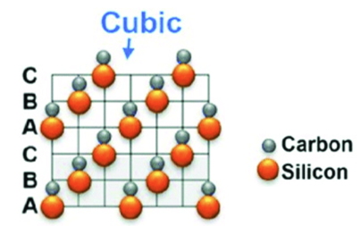
Figure 2 Schematic diagram of CVD
Sublimation epitaxy (SE) method: Figure 3 is an experimental structure diagram of the SE method for preparing 3C-SiC. The main steps are the decomposition and sublimation of the SiC source in the high temperature zone, the transportation of the sublimates, and the reaction and crystallization of the sublimates on the substrate surface at a lower temperature. The details are as follows: 6H-SiC or 4H-SiC substrate is placed on the top of the crucible, and high-purity SiC powder is used as SiC raw material and placed at the bottom of the graphite crucible. The crucible is heated to 1900-2100℃ by radio frequency induction, and the substrate temperature is controlled to be lower than the SiC source, forming an axial temperature gradient inside the crucible, so that the sublimated SiC material can condense and crystallize on the substrate to form 3C-SiC heteroepitaxial.
The advantages of sublimation epitaxy are mainly in two aspects: 1. The epitaxy temperature is high, which can reduce crystal defects; 2. It can be etched to obtain an etched surface at the atomic level. However, during the growth process, the reaction source cannot be adjusted, and the silicon-carbon ratio, time, various reaction sequences, etc. cannot be changed, resulting in a decrease in the controllability of the growth process.
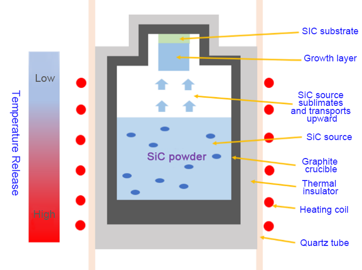
Figure 3 Schematic diagram of SE method for growing 3C-SiC epitaxy
Molecular beam epitaxy (MBE) is an advanced thin film growth technology, which is suitable for growing 3C-SiC epitaxial layers on 4H-SiC or 6H-SiC substrates. The basic principle of this method is: in an ultra-high vacuum environment, through precise control of the source gas, the elements of the growing epitaxial layer are heated to form a directional atomic beam or molecular beam and incident on the heated substrate surface for epitaxial growth. The common conditions for growing 3C-SiC epitaxial layers on 4H-SiC or 6H-SiC substrates are: under silicon-rich conditions, graphene and pure carbon sources are excited into gaseous substances with an electron gun, and 1200-1350℃ is used as the reaction temperature. 3C-SiC heteroepitaxial growth can be obtained at a growth rate of 0.01-0.1 nms-1 [13].
Conclusion and Prospect
Through continuous technological progress and in-depth mechanism research, 3C-SiC heteroepitaxial technology is expected to play a more important role in the semiconductor industry and promote the development of high-efficiency electronic devices. For example, continuing to explore new growth techniques and strategies, such as introducing HCl atmosphere to increase the growth rate while maintaining low defect density, is the direction of future research; in-depth research on the defect formation mechanism, and the development of more advanced characterization techniques, such as photoluminescence and cathodoluminescence analysis, to achieve more precise defect control and optimize material properties; rapid growth of high-quality thick film 3C-SiC is the key to meeting the needs of high-voltage devices, and further research is needed to overcome the balance between growth rate and material uniformity; combined with the application of 3C-SiC in heterogeneous structures such as SiC/GaN, explore its potential applications in new devices such as power electronics, optoelectronic integration and quantum information processing.
References:
[1] Nishino S , Hazuki Y , Matsunami H ,et al. Chemical Vapor Deposition of Single Crystalline β‐SiC Films on Silicon Substrate with Sputtered SiC Intermediate Layer[J].Journal of The Electrochemical Society, 1980, 127(12):2674-2680.
[2]叶志镇,王亚东,黄靖云,等.低温生长硅基碳化硅薄膜研究[J].真空科学与技术学报, 2002, 022(001):58-60.
[3]安霞,庄惠照,李怀祥,等.在(111)Si衬底上磁控溅射法制备纳米SiC薄膜[J].山东师范大学学报:自然科学版, 2001: 382-384..
[4] Seki K, Alexander, Kozawa S, et al. Polytype-selective growth of SiC by supersaturation control in solution growth[J]. Journal of Crystal Growth, 2012, 360:176-180.
[5] 陈尧,赵富强,朱炳先,贺帅.国内外碳化硅功率器件发展综述[J].车辆与动力技术,2020:49-54.
[6] Li X , Wang G .CVD growth of 3C-SiC layers on 4H-SiC substrates with improved morphology[J].Solid State Communications, 2023:371.
[7] 侯凯文. Si 图形化衬底研究及其在 3C-SiC 生长上的应用[D]. 西安理工大学, 2018.
[8]Lars, Hiller , Thomas, et al. Hydrogen Effects in ECR-Etching of 3C-SiC(100) Mesa Structures[J].Materials Science Forum, 2014.
[9]徐青芳.激光化学气相沉积法制备-3C-SiC薄膜[D].武汉理工大学,2016.
[10] Foisal A R M , Nguyen T , Dinh T K ,et al.3C-SiC/Si Heterostructure: An Excellent Platform for Position-Sensitive Detectors Based on Photovoltaic Effect[J].ACS Applied Materials & Interfaces, 2019: 40980-40987.
[11] 辛斌. 基于CVD工艺的3C/4H-SiC异质外延:缺陷表征及演化[D].西安电子科技大学.
[12] 董林. 碳化硅大面积多片外延生长技术及物性表征[D].中国科学院大学, 2014.
[13] Diani M , Simon L , Kubler L ,et al. Crystal growth of 3C-SiC polytype on 6H-SiC(0001) substrate[J]. Journal of Crystal Growth, 2002, 235(1):95-102.
Previous:ALD Atomic Layer Deposition Recipe


