
- English
- Español
- Português
- русский
- Français
- 日本語
- Deutsch
- tiếng Việt
- Italiano
- Nederlands
- ภาษาไทย
- Polski
- 한국어
- Svenska
- magyar
- Malay
- বাংলা ভাষার
- Dansk
- Suomi
- हिन्दी
- Pilipino
- Türkçe
- Gaeilge
- العربية
- Indonesia
- Norsk
- تمل
- český
- ελληνικά
- український
- Javanese
- فارسی
- தமிழ்
- తెలుగు
- नेपाली
- Burmese
- български
- ລາວ
- Latine
- Қазақша
- Euskal
- Azərbaycan
- Slovenský jazyk
- Македонски
- Lietuvos
- Eesti Keel
- Română
- Slovenski
- मराठी
- Srpski језик
Chip manufacturing: A process flow of MOSFET
2024-07-31
The chip manufacturing process includes photolithography,etching, diffusion, thin film, ion implantation, chemical mechanical polishing, cleaning, etc.This article roughly explains how these processes are integrated in sequence to manufacture a MOSFET.
1.We first have a substrate with a silicon purity of up to 99.9999999%.
![]()
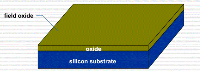
2. Grow a layer of oxide film on the silicon crystal substrate.
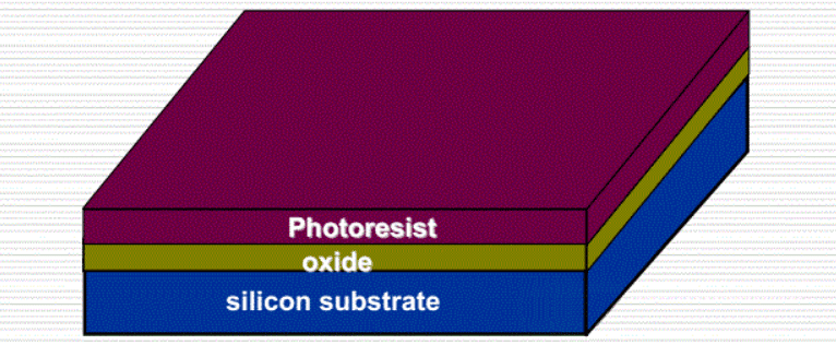
3. Spin-coat photoresist evenly.
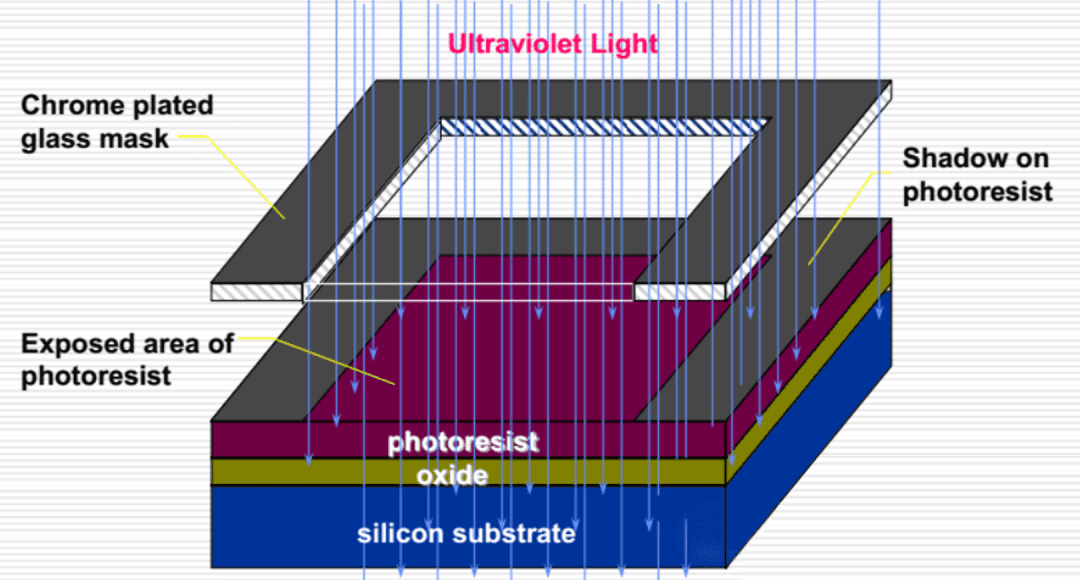
4.Photolithography is performed through a photomask to transfer the pattern on the photomask to the photoresist.
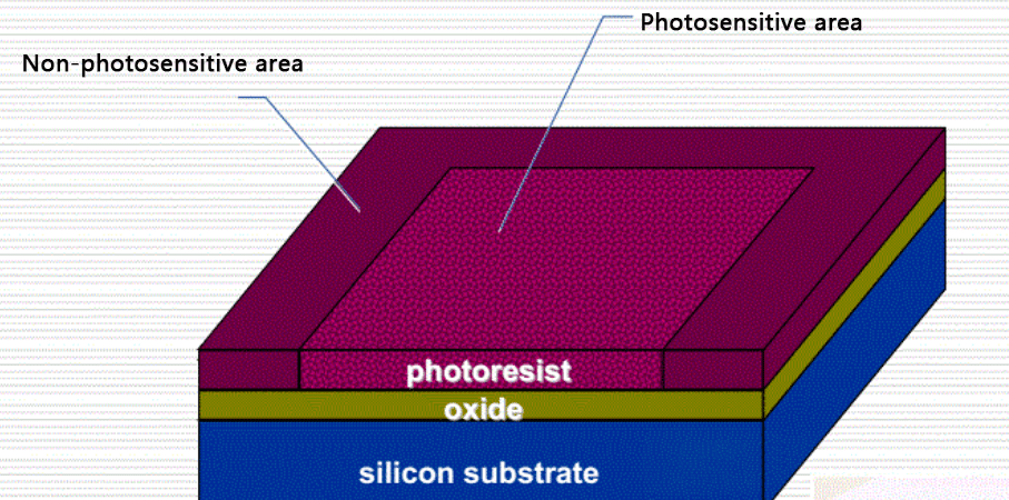
5. The photoresist in the photosensitive area is washed away after development.
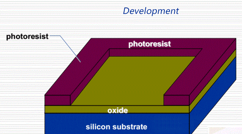
6. Etch away the oxide film that is not covered by the photoresist through etching, so that the photolithography pattern is transferred to the wafer.
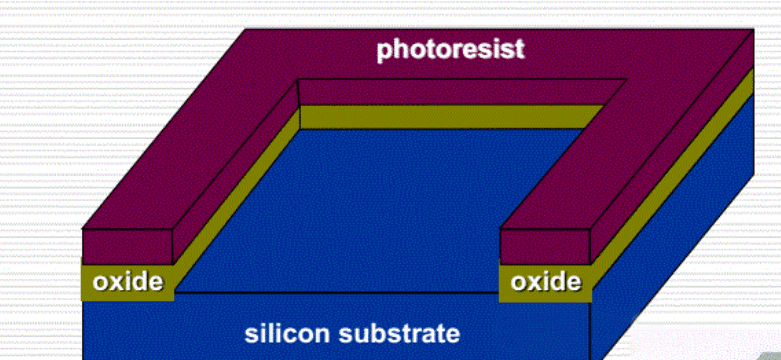
7. Clean and remove the excess photoresist.
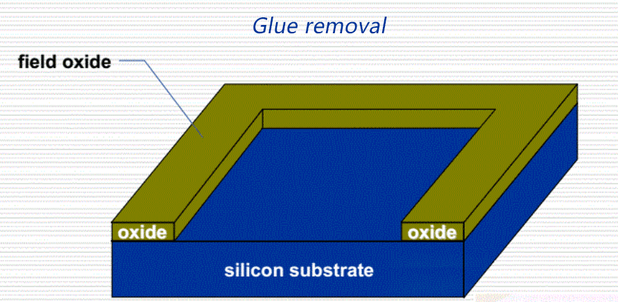
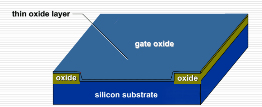
8. Apply another thinner oxide film. After that, through the above photolithography and etching, only the oxide film in the gate area is retained.
9. Grow a layer of polysilicon on it
![]()
10. As in step 7, use photolithography and etching to keep only the polysilicon on the gate oxide layer.
![]()
11.Cover the oxide layer and gate by photolithography cleaning, so that the entire wafer is ion-implanted, and there will be a source and drain.
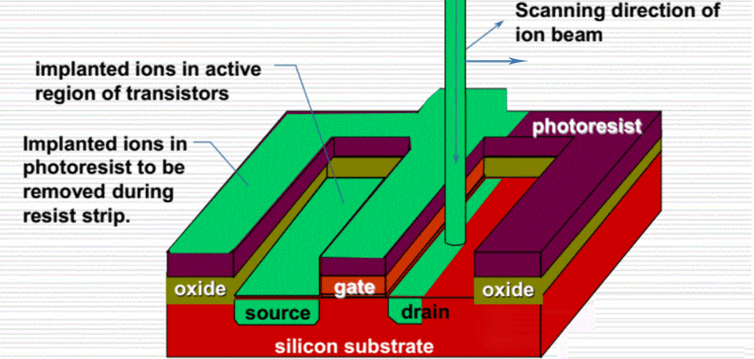
![]()
12. Grow a layer of insulating film on the wafer.
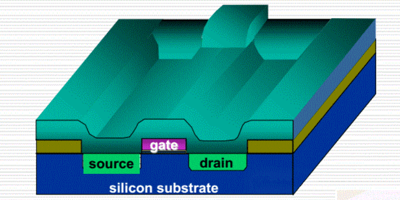
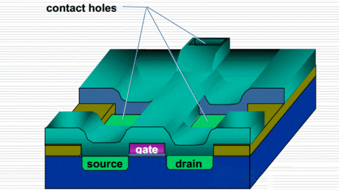
13. Etch the contact holes of the source, gate and drain by photolithography and etching.
14. Then deposit metal in the etched area, so that there will be conductive metal wires for the source, gate and drain.
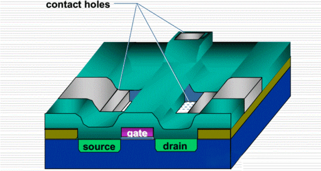
Finally, a complete MOSFET is manufactured through a combination of various processes.
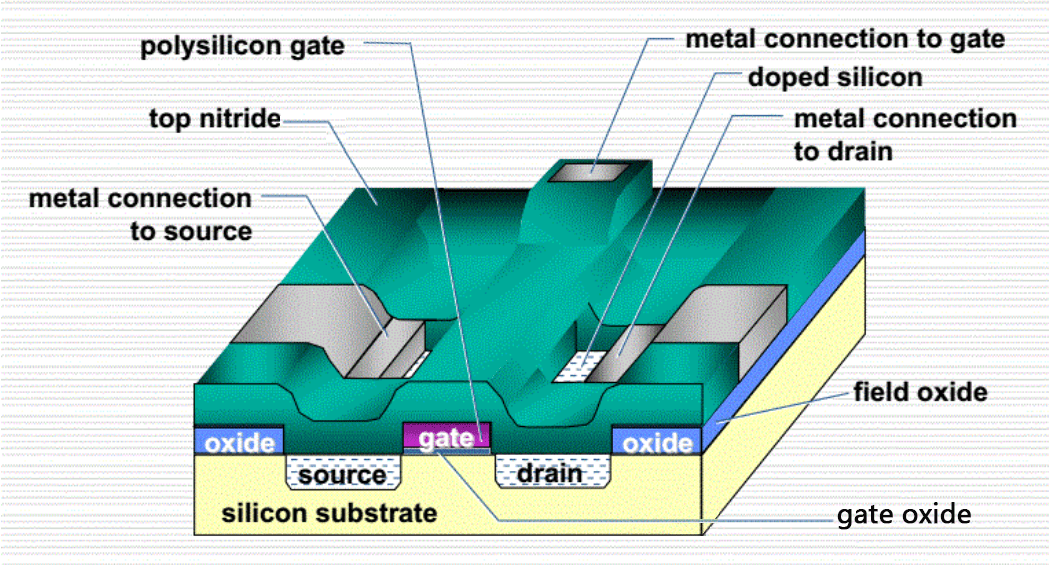
In fact, the bottom layer of the chip is composed of a large number of transistors.
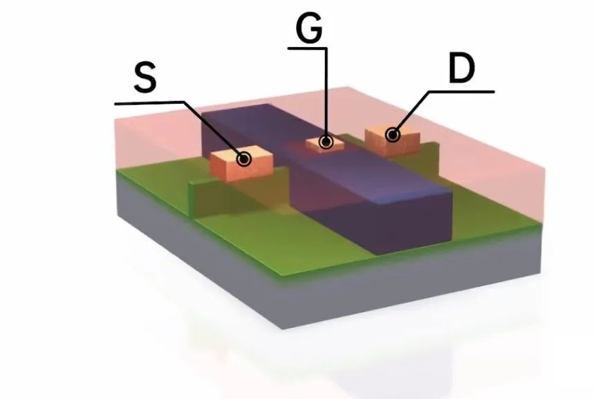
MOSFET manufacturing diagram, source, gate, drain
![]()
Various transistors form logic gates
![]()
Logic gates form arithmetic units
![]()
Finally, it is a chip the size of a fingernail
![]()


