- English
- Español
- Português
- русский
- Français
- 日本語
- Deutsch
- tiếng Việt
- Italiano
- Nederlands
- ภาษาไทย
- Polski
- 한국어
- Svenska
- magyar
- Malay
- বাংলা ভাষার
- Dansk
- Suomi
- हिन्दी
- Pilipino
- Türkçe
- Gaeilge
- العربية
- Indonesia
- Norsk
- تمل
- český
- ελληνικά
- український
- Javanese
- فارسی
- தமிழ்
- తెలుగు
- नेपाली
- Burmese
- български
- ລາວ
- Latine
- Қазақша
- Euskal
- Azərbaycan
- Slovenský jazyk
- Македонски
- Lietuvos
- Eesti Keel
- Română
- Slovenski
- मराठी
- Srpski језик
Ion Beam Sputter sources grid
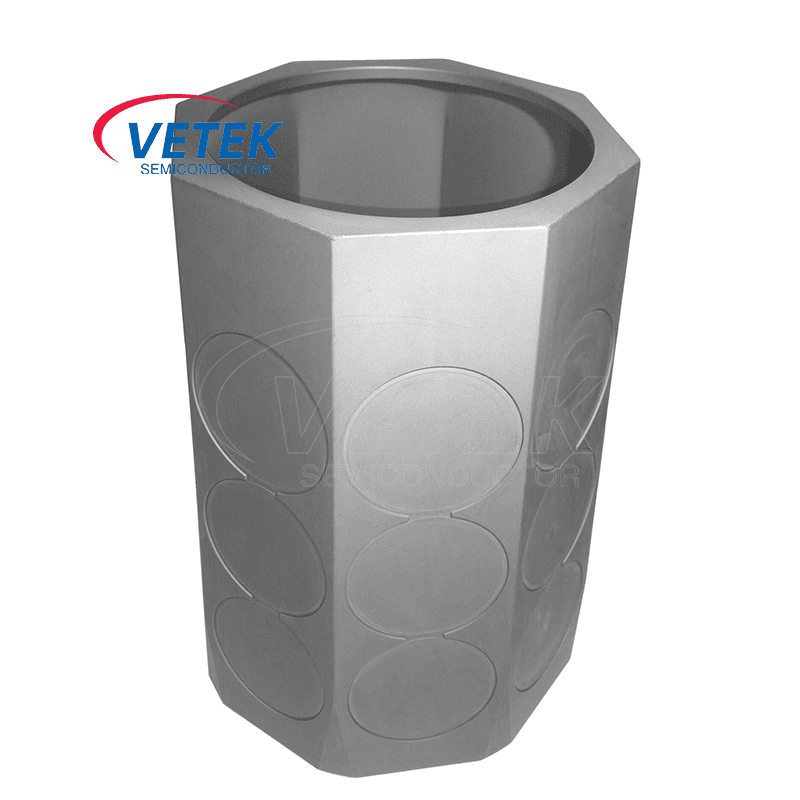
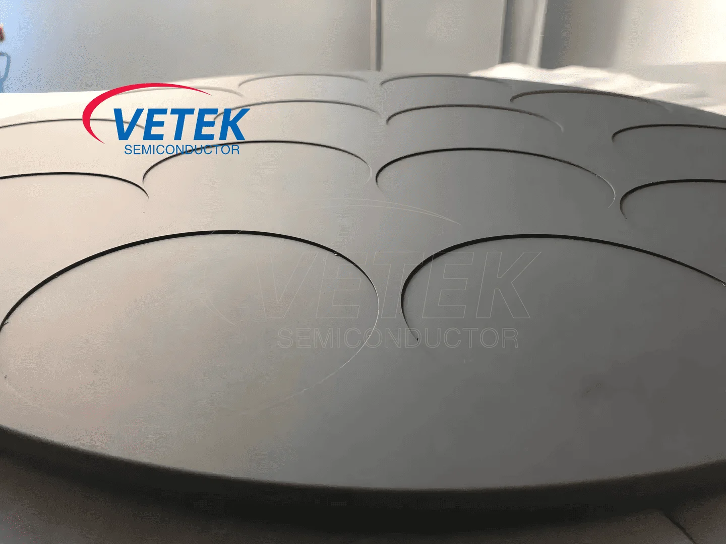
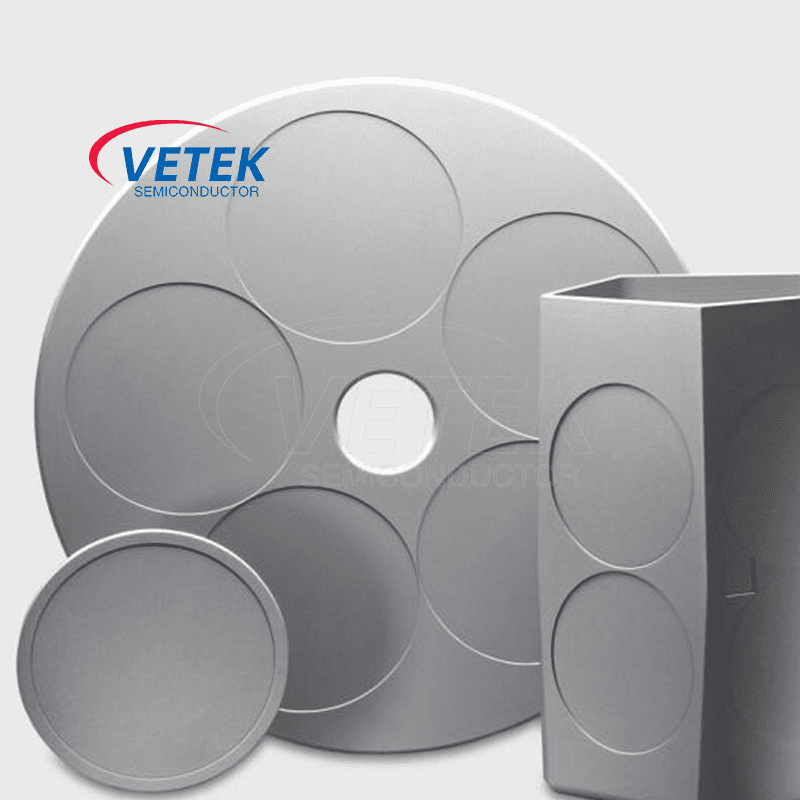
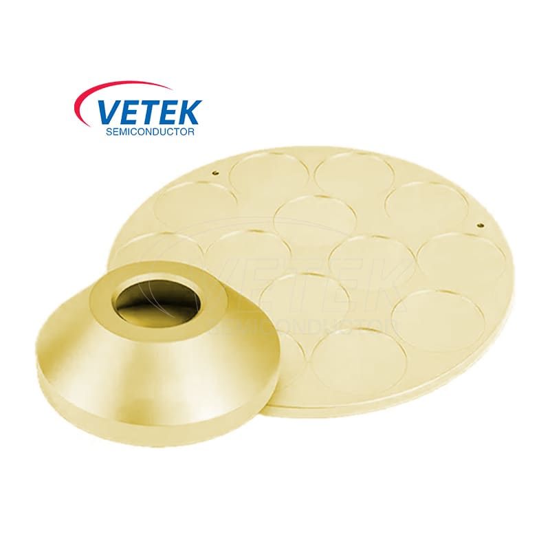
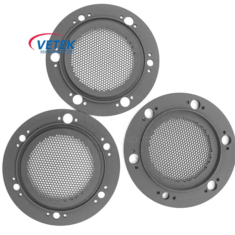
Ion beam is mainly used for ion etching, ion coating and plasma injection. The role of the Ion Beam Sputter sources grid is to dissect the ions and accelerate them to the required energy. Vetek Semiconductor provides high purity graphite ion beam Ion Beam Sputter sources grid for optical lens ion beam polishing, semiconductor wafer modification, etc. Welcome to inquire about customized products.
Send Inquiry
An ion beam source is a Plasma source fitted with a grid and capable of extracting ions. The OIPT (Oxford Instruments Plasma Technology) ion beam source consists of three main components: a discharge chamber, a grid, and a neutralizer.
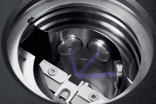
The Schematic diagram of the Ion Beam Sputter sources grid working
● The discharge chamber is a quartz or aluminum chamber surrounded by a radio-frequency antenna. Its effect is to ionize gas (usually argon) through a radio-frequency field, producing plasma. The radio-frequency field excites the free electrons, causing the gas atoms to split into ions and electrons, which in turn produces plasma. The end to end voltage of the RF antenna in the discharge chamber is very high, which has an electrostatic effect on the ions, making them high energy ions.
● The role of the grid in the ion source is to dissect the ions and accelerate them to the required energy. The grid of OIPT ion beam source is composed of 2~3 grids with a specific layout pattern, which can form a wide ion beam. The design features of the grid include spacing and curvature, which can be adjusted according to application requirements to control the energy of the ions.
● A neutralizer is an electron source used to neutralize the ionic charge in the ion beam, reduce the divergence of the ion beam, and prevent charging on the surface of the chip or sputtering target. Optimize the interaction between the neutralizer and other parameters to balance the various parameters for the desired result. The divergence of the ion beam is affected by several parameters, including gas scattering and various voltage and current parameters.
The process of OIPT ion beam source is improved by placing electrostatic screen in quartz chamber and adopting three-grid structure. The electrostatic screen prevents the electrostatic field from entering the ion source and effectively prevents the deposition of the internal conductive layer. The three-grid structure includes shielding grid, accelerating grid and decelerating grid, which can precisely define the energy and drive the ions to improve the collimation and efficiency of the ion.
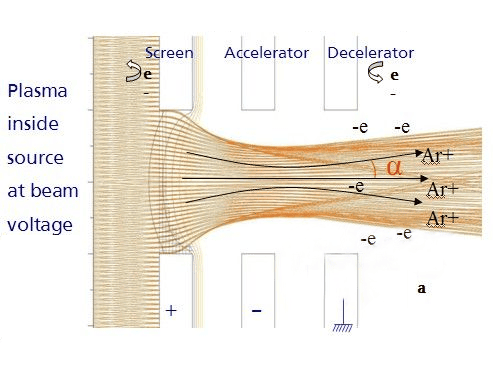
Figure 1. Plasma inside source at beam voltage
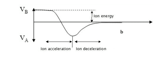
Figure2. Plasma inside source at beam voltage
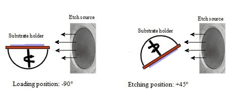
Figure 3. Schematic diagram of ion beam etching and deposition system
Etching techniques primarily fall into two categories:
● Ion Beam Etching with Inert Gases (IBE): This method involves using inert gases such as argon, xenon, neon, or krypton for etching. IBE provides physical etching and allows processing of metals like gold, platinum, and palladium, which are typically unsuitable for reactive ion etching. For multilayer materials, IBE is the preferred method due to its simplicity and efficiency, as seen in the production of devices like Magnetic Random Access Memory (MRAM).
● Reactive Ion Beam Etching (RIBE): RIBE entails the addition of chemical reactive gases such as SF6, CHF3, CF4, O2, or Cl2 to inert gases like argon. This technique enhances etching rates and material selectivity by introducing chemical reactivity. RIBE can be introduced either through the etching source or through an environment surrounding the chip on the substrate platform. The latter method, known as Chemically Assisted Ion Beam Etching (CAIBE), provides higher efficiency and allows for controlled etching characteristics.
Ion beam etching offers a range of advantages in the realm of material processing. It excels in its capacity to etch diverse materials, extending even to those traditionally challenging for plasma etching techniques. Furthermore, the method allows for the shaping of sidewall profiles through sample tilting, enhancing the precision of the etching process. By introducing chemical reactive gases, ion beam etching can significantly boost etch rates, providing a means to expedite material removal.
The technology also grants independent control over critical parameters such as ion beam current and energy, facilitating tailored and precise etching processes. Notably, ion beam etching boasts exceptional operational repeatability, ensuring consistent and reliable results. Additionally, it showcases remarkable etch uniformity, crucial for achieving consistent material removal across surfaces. With its broad process flexibility, ion beam etching stands as a versatile and powerful tool in material fabrication and microfabrication applications.
Why is Vetek Semiconductor graphite material suitable for making ion beam grids?
● Conductivity: Graphite exhibits excellent conductivity, which is crucial for ion beam grids to effectively guide ion beams for acceleration or deceleration.
● Chemical Stability: Graphite is chemically stable, capable of resisting chemical erosion and corrosion, thus maintaining structural integrity and performance stability.
● Mechanical Strength: Graphite possesses sufficient mechanical strength and stability to withstand the forces and pressures that may arise during ion beam acceleration.
● Temperature Stability: Graphite demonstrates good stability at high temperatures, enabling it to withstand high-temperature environments within ion beam equipment without failure or deformation.
VeTek Semiconductor Ion Beam Sputter sources grid products:
![]()

