- English
- Español
- Português
- русский
- Français
- 日本語
- Deutsch
- tiếng Việt
- Italiano
- Nederlands
- ภาษาไทย
- Polski
- 한국어
- Svenska
- magyar
- Malay
- বাংলা ভাষার
- Dansk
- Suomi
- हिन्दी
- Pilipino
- Türkçe
- Gaeilge
- العربية
- Indonesia
- Norsk
- تمل
- český
- ελληνικά
- український
- Javanese
- فارسی
- தமிழ்
- తెలుగు
- नेपाली
- Burmese
- български
- ລາວ
- Latine
- Қазақша
- Euskal
- Azərbaycan
- Slovenský jazyk
- Македонски
- Lietuvos
- Eesti Keel
- Română
- Slovenski
- मराठी
- Srpski језик
4°off axis p-type SiC Wafer
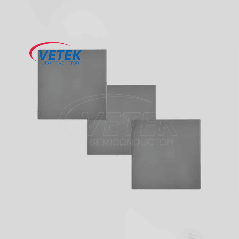
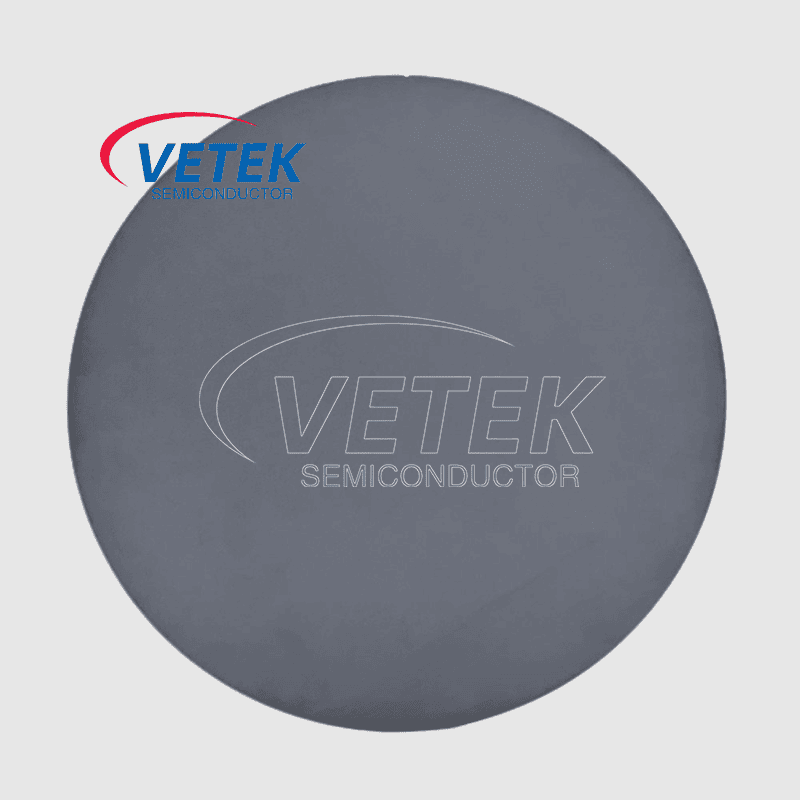
VeTek Semiconductor is a professional Chinese manufacturer of 4°off axis p-type SiC Wafer, 4H N type SiC Substrate, and 4H Semi Insulating type SiC Substrate. Among them, 4°off axis p-type SiC Wafer is a special semiconductor material used in high-performance electronic devices. VeTek Semiconductor is committed to providing advanced solutions for various SiC Wafer products for the semiconductor industry. We sincerely look forward to your further consultation.
Send Inquiry
As a professional semiconductor manufacturer in China, VeTek Semiconductor 4°off axis p-type SiC Wafer refers to 4H silicon carbide (SiC) wafers that deviate 4° from the main crystal direction of the crystal (usually the c-axis) when cutting and undergo P-type doping. This product is usually used in the manufacture of power electronic devices and radio frequency (RF) devices in the semiconductor industry chain, and has excellent product advantages.
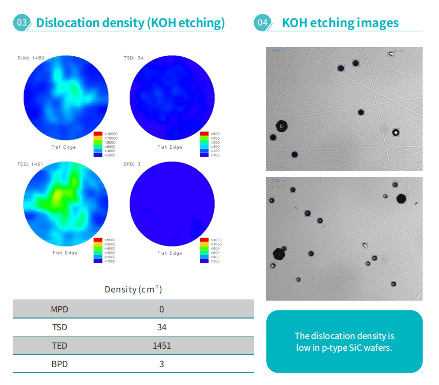
Through off-axis cutting, VeTek Semiconductor's 4°off axis p-type SiC Wafer can effectively reduce dislocations and defects generated during the growth of the epitaxial layer, thereby improving the quality of the wafer. In addition, the 4° Off-Axis orientation helps to grow a more uniform and defect-free epitaxial layer, improves the quality of the epitaxial layer, and is generally suitable for the manufacture of high-performance devices.
Moreover, VeTek Semiconductor's 4°off axis p-type SiC Wafer products can make the wafer have more hole carriers and form a P-type semiconductor by doping acceptor impurities (such as aluminum or boron). P-type 4H-SiC wafers are often used in the manufacture of power devices that require a P-type layer. This type of semiconductor has excellent electrical properties.
Compared with other polymorphs such as 6H-SiC, 4H-SiC has higher electron mobility and breakdown electric field strength, and is suitable for high-frequency and high-power scenarios. In addition, 4H-SiC materials have excellent high-voltage and high-temperature resistance, and can work normally in harsh environments.
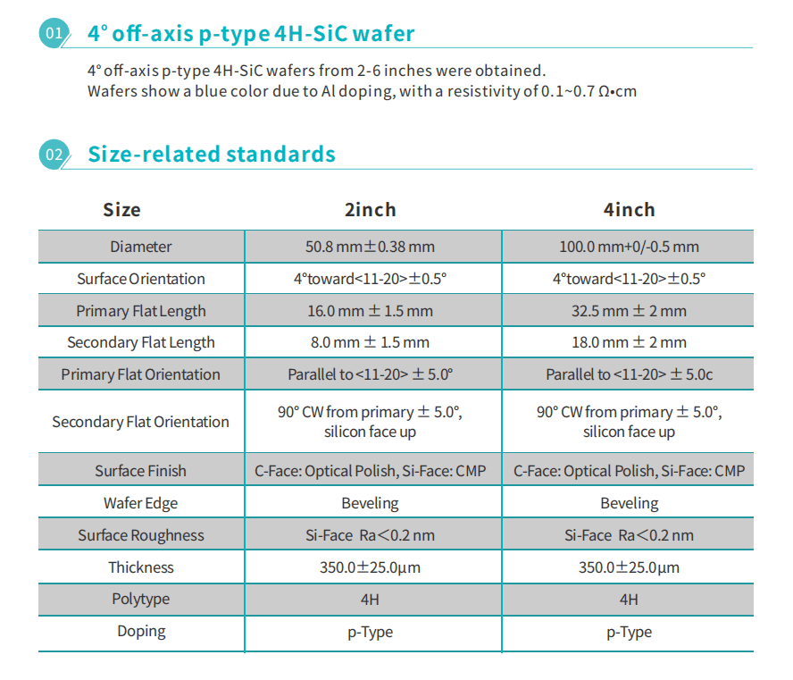
2inch 4inch 4°off axis p-type SiC Wafer Size-related standards:
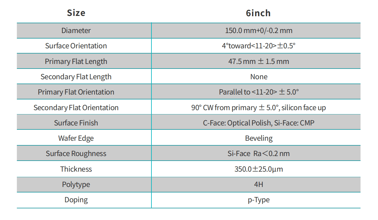
6 inch 4°off axis p-type SiC Wafer Size-related standards:
4°off axis p-type SiC Wafer Detection methods and terminology:
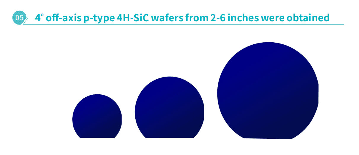
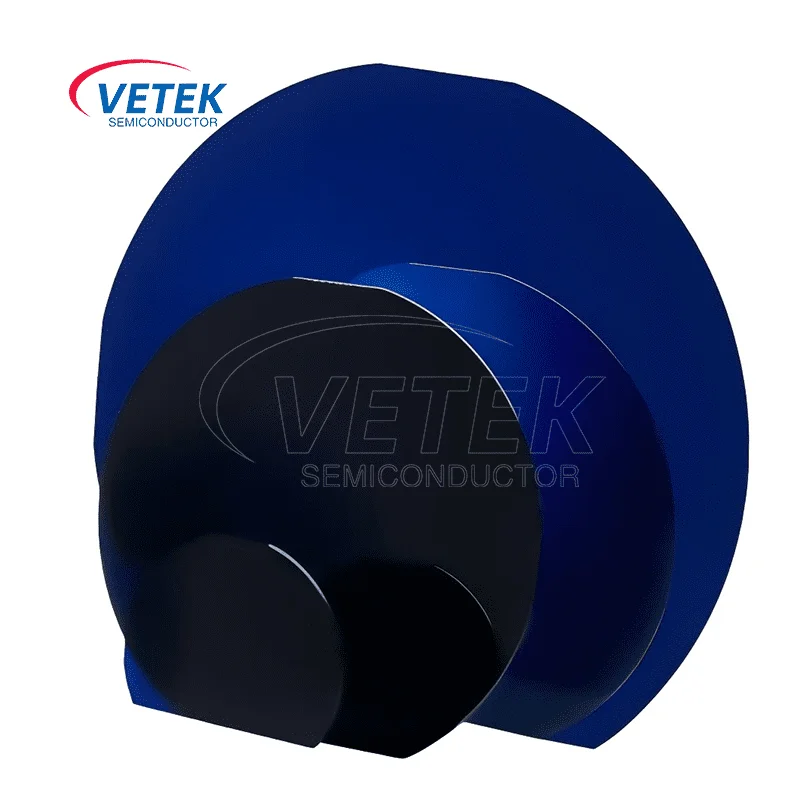
VeTek Semiconductor already has 4° off axis p-type 4H-SiC substrates from 2~6 inches. The substrate is doped with aluminum and appears blue. The resistivity ranges from 0.1 to 0.7Ω•cm.
If you have product requirements for 4° off axis p-type SiC Wafer,welcome to consult us.
