
- English
- Español
- Português
- русский
- Français
- 日本語
- Deutsch
- tiếng Việt
- Italiano
- Nederlands
- ภาษาไทย
- Polski
- 한국어
- Svenska
- magyar
- Malay
- বাংলা ভাষার
- Dansk
- Suomi
- हिन्दी
- Pilipino
- Türkçe
- Gaeilge
- العربية
- Indonesia
- Norsk
- تمل
- český
- ελληνικά
- український
- Javanese
- فارسی
- தமிழ்
- తెలుగు
- नेपाली
- Burmese
- български
- ລາວ
- Latine
- Қазақша
- Euskal
- Azərbaycan
- Slovenský jazyk
- Македонски
- Lietuvos
- Eesti Keel
- Română
- Slovenski
- मराठी
- Srpski језик

Silicon carbide nanomaterials
2024-08-19
Silicon carbide nanomaterials
Silicon carbide nanomaterials (SiC nanomaterials) refer to materials composed of silicon carbide (SiC) with at least one dimension in the nanometer scale (usually defined as 1-100nm) in three-dimensional space. Silicon carbide nanomaterials can be classified into zero-dimensional, one-dimensional, two-dimensional and three-dimensional structures according to their structure.
Zero-dimensional nanostructures are structures whose all dimensions are on the nanometer scale, mainly including solid nanocrystals, hollow nanospheres, hollow nanocages and core-shell nanospheres.
One-dimensional nanostructures refer to structures in which two dimensions are confined to the nanometer scale in three-dimensional space. This structure has many forms, including nanowires (solid center), nanotubes (hollow center), nanobelts or nanobelts (narrow rectangular cross-section) and nanoprisms (prism-shaped cross-section). This structure has become the focus of intensive research due to its unique applications in mesoscopic physics and nanoscale device manufacturing. For example, carriers in one-dimensional nanostructures can only propagate in one direction of the structure (i.e., the longitudinal direction of the nanowire or nanotube), and can be used as interconnects and key devices in nanoelectronics.
Two-dimensional nanostructures, which have only one dimension at the nanoscale, usually perpendicular to their layer plane, such as nanosheets, nanosheets, nanosheets and nanospheres, have received special attention recently, not only for the basic understanding of their growth mechanism, but also for exploring their potential applications in light emitters, sensors, solar cells, etc.
Three-dimensional nanostructures are usually called complex nanostructures, which are formed by a collection of one or more basic structural units in zero-dimensional, one-dimensional, and two-dimensional (such as nanowires or nanorods connected by single crystal junctions), and their overall geometric dimensions are on the nanometer or micrometer scale. Such complex nanostructures with high surface area per unit volume provide many advantages, such as long optical paths for efficient light absorption, fast interfacial charge transfer, and tunable charge transport capabilities. These advantages enable three-dimensional nanostructures to advance design in future energy conversion and storage applications. From 0D to 3D structures, a wide variety of nanomaterials have been studied and gradually introduced into industry and daily life.
Synthesis methods of SiC nanomaterials
Zero-dimensional materials can be synthesized by hot melt method, electrochemical etching method, laser pyrolysis method, etc. to obtain SiC solid nanocrystals ranging from a few nanometers to tens of nanometers, but are usually pseudo-spherical, as shown in Figure 1.
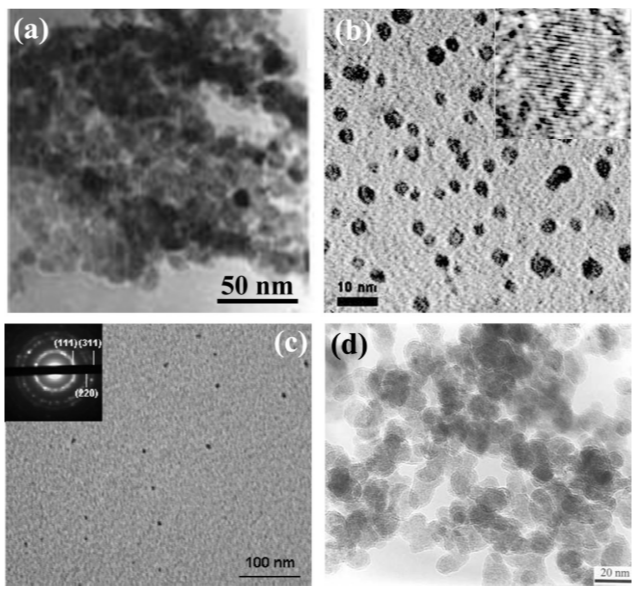
Figure 1 TEM images of β-SiC nanocrystals prepared by different methods
(a) Solvothermal synthesis[34]; (B) Electrochemical etching method[35]; (c) Thermal processing[48]; (d) Laser pyrolysis[49]
Dasog et al. synthesized spherical β-SiC nanocrystals with controllable size and clear structure by solid-state double decomposition reaction between SiO2, Mg and C powders[55], as shown in Figure 2.
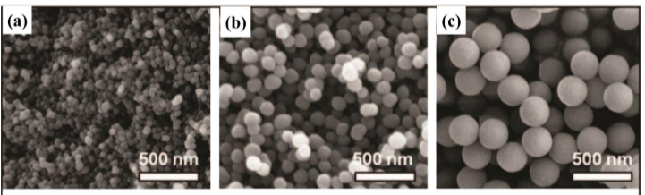
Figure 2 FESEM images of spherical SiC nanocrystals with different diameters[55]
(a) 51.3 ± 5.5 nm; (B) 92.8 ± 6.6 nm; (c) 278.3 ± 8.2 nm
Vapor phase method for growing SiC nanowires. Gas phase synthesis is the most mature method for forming SiC nanowires. In a typical process, vapor substances used as reactants to form the final product are generated by evaporation, chemical reduction and gaseous reaction (requiring high temperature). Although high temperature increases additional energy consumption, the SiC nanowires grown by this method usually have high crystal integrity, clear nanowires/nanorods, nanoprisms, nanoneedles, nanotubes, nanobelts, nanocables, etc., as shown in Figure 3.
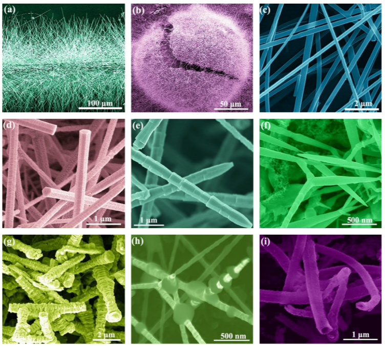
Figure 3 Typical morphologies of one-dimensional SiC nanostructures
(a) Nanowire arrays on carbon fibers; (b) Ultralong nanowires on Ni-Si balls; (c) Nanowires; (d) Nanoprisms; (e) Nanobamboo; (f) Nanoneedles; (g) Nanobones; (h) Nanochains; (i) Nanotubes
Solution method for the preparation of SiC nanowires. The solution method is used to prepare SiC nanowires, which reduces the reaction temperature. The method may include crystallizing a solution phase precursor through spontaneous chemical reduction or other reactions at a relatively mild temperature. As representatives of the solution method, solvothermal synthesis and hydrothermal synthesis have been commonly used to obtain SiC nanowires at low temperatures.
Two-dimensional nanomaterials can be prepared by solvothermal methods, pulsed lasers, carbon thermal reduction, mechanical exfoliation, and microwave plasma enhanced CVD. Ho et al. realized a 3D SiC nanostructure in the shape of a nanowire flower, as shown in Figure 4. The SEM image shows that the flower-like structure has a diameter of 1-2 μm and a length of 3-5 μm.
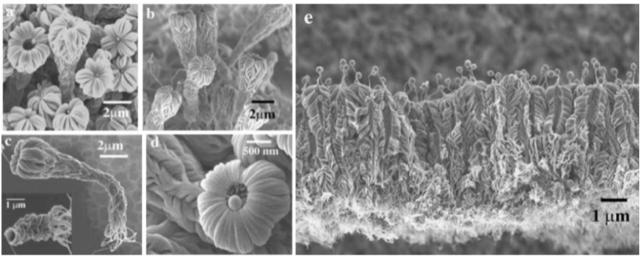
Figure 4 SEM image of a three-dimensional SiC nanowire flower
Performance of SiC nanomaterials
SiC nanomaterials are an advanced ceramic material with excellent performance, which has good physical, chemical, electrical and other properties.
✔ Physical properties
High hardness: The microhardness of nano-silicon carbide is between corundum and diamond, and its mechanical strength is higher than that of corundum. It has high wear resistance and good self-lubrication.
High thermal conductivity: Nano-silicon carbide has excellent thermal conductivity and is an excellent thermal conductive material.
Low thermal expansion coefficient: This allows nano-silicon carbide to maintain a stable size and shape under high temperature conditions.
High specific surface area: One of the characteristics of nanomaterials, it is conducive to improving its surface activity and reaction performance.
✔ Chemical properties
Chemical stability: Nano-silicon carbide has stable chemical properties and can maintain its performance unchanged under various environments.
Antioxidation: It can resist oxidation at high temperatures and exhibits excellent high temperature resistance.
✔Electrical properties
High bandgap: The high bandgap makes it an ideal material for making high-frequency, high-power, and low-energy electronic devices.
High electron saturation mobility: It is conducive to the rapid transmission of electrons.
✔Other characteristics
Strong radiation resistance: It can maintain stable performance in a radiation environment.
Good mechanical properties: It has excellent mechanical properties such as high elastic modulus.
Application of SiC nanomaterials
Electronics and semiconductor devices: Due to its excellent electronic properties and high-temperature stability, nano-silicon carbide is widely used in high-power electronic components, high-frequency devices, optoelectronic components and other fields. At the same time, it is also one of the ideal materials for manufacturing semiconductor devices.
Optical applications: Nano-silicon carbide has a wide bandgap and excellent optical properties, and can be used to manufacture high-performance lasers, LEDs, photovoltaic devices, etc.
Mechanical parts: Taking advantage of its high hardness and wear resistance, nano-silicon carbide has a wide range of applications in the manufacture of mechanical parts, such as high-speed cutting tools, bearings, mechanical seals, etc., which can greatly improve the wear resistance and service life of the parts.
Nanocomposite materials: Nano-silicon carbide can be combined with other materials to form nanocomposites to improve the mechanical properties, thermal conductivity and corrosion resistance of the material. This nanocomposite material is widely used in aerospace, automotive industry, energy field, etc.
High temperature structural materials: Nano silicon carbide has excellent high temperature stability and corrosion resistance, and can be used in extreme high temperature environments. Therefore, it is used as a high temperature structural material in aerospace, petrochemical, metallurgy and other fields, such as manufacturing high temperature furnaces, furnace tubes, furnace linings, etc.
Other applications: Nano silicon carbide is also used in hydrogen storage, photocatalysis and sensing, showing broad application prospects.


