
- English
- Español
- Português
- русский
- Français
- 日本語
- Deutsch
- tiếng Việt
- Italiano
- Nederlands
- ภาษาไทย
- Polski
- 한국어
- Svenska
- magyar
- Malay
- বাংলা ভাষার
- Dansk
- Suomi
- हिन्दी
- Pilipino
- Türkçe
- Gaeilge
- العربية
- Indonesia
- Norsk
- تمل
- český
- ελληνικά
- український
- Javanese
- فارسی
- தமிழ்
- తెలుగు
- नेपाली
- Burmese
- български
- ລາວ
- Latine
- Қазақша
- Euskal
- Azərbaycan
- Slovenský jazyk
- Македонски
- Lietuvos
- Eesti Keel
- Română
- Slovenski
- मराठी
- Srpski језик

What is semiconductor epitaxy process?
2024-08-13
It is ideal to build integrated circuits or semiconductor devices on a perfect crystalline base layer. The epitaxy (epi) process in semiconductor manufacturing aims to deposit a fine single-crystalline layer, usually about 0.5 to 20 microns, on a single-crystalline substrate. The epitaxy process is an important step in the manufacture of semiconductor devices, especially in silicon wafer manufacturing.
Epitaxy (epi) process in semiconductor manufacturing
| Overview of Epitaxy in Semiconductor Manufacturing | |
| What is it | The epitaxy (epi) process in semiconductor manufacturing allows the growth of a thin crystalline layer in a given orientation on top of a crystalline substrate. |
| Goal | In semiconductor manufacturing, the goal of the epitaxy process is to make the electrons transport more efficiently through the device. In the construction of semiconductor devices, epitaxy layers are included to refine and make the structure uniform. |
| Process | The epitaxy process allows the growth of higher purity epitaxial layers on a substrate of the same material. In some semiconductor materials, such as heterojunction bipolar transistors (HBTs) or metal oxide semiconductor field effect transistors (MOSFETs), the epitaxy process is used to grow a layer of material different from the substrate. It is the epitaxy process that makes it possible to grow a low density doped layer on a layer of highly doped material. |
Overview of Epitaxy in Semiconductor Manufacturing
What is it The epitaxy (epi) process in semiconductor manufacturing allows the growth of a thin crystalline layer in a given orientation on top of a crystalline substrate.
Goal In semiconductor manufacturing, the goal of the epitaxy process is to make the electrons transport more efficiently through the device. In the construction of semiconductor devices, epitaxy layers are included to refine and make the structure uniform.
Process The epitaxy process allows the growth of higher purity epitaxial layers on a substrate of the same material. In some semiconductor materials, such as heterojunction bipolar transistors (HBTs) or metal oxide semiconductor field effect transistors (MOSFETs), the epitaxy process is used to grow a layer of material different from the substrate. It is the epitaxy process that makes it possible to grow a low density doped layer on a layer of highly doped material.
Overview of epitaxy process in semiconductor manufacturing
What it is The epitaxy (epi) process in semiconductor manufacturing allows the growth of a thin crystalline layer in a given orientation on top of a crystalline substrate.
Goal in semiconductor manufacturing, the goal of the epitaxy process is to make the electrons transported through the device more efficiently. In the construction of semiconductor devices, epitaxy layers are included to refine and make the structure uniform.
The epitaxy process allows the growth of higher purity epitaxial layers on a substrate of the same material. In some semiconductor materials, such as heterojunction bipolar transistors (HBTs) or metal oxide semiconductor field effect transistors (MOSFETs), the epitaxy process is used to grow a layer of material different from the substrate. It is the epitaxy process that makes it possible to grow a low-density doped layer on a layer of highly doped material.
Types of Epitaxial Processes in Semiconductor Manufacturing
In the epitaxial process, the direction of growth is determined by the underlying substrate crystal. Depending on the repetition of the deposition, there can be one or more epitaxial layers. Epitaxial processes can be used to form thin layers of material that is the same or different in chemical composition and structure from the underlying substrate.
| Two types of Epi processes | ||
| Characteristics | Homoepitaxy | Heteroepitaxy |
| Growth layers | The epitaxial growth layer is the same material as the substrate layer | The epitaxial growth layer is a different material from the substrate layer |
| Crystal structure and lattice | The crystal structure and lattice constant of the substrate and epitaxial layer are the same | The crystal structure and lattice constant of the substrate and epitaxial layer are different |
| Examples | Epitaxial growth of high-purity silicon on silicon substrate | Epitaxial growth of gallium arsenide on silicon substrate |
| Applications | Semiconductor device structures requiring layers of different doping levels or pure films on less pure substrates | Semiconductor device structures requiring layers of different materials or building crystalline films of materials that cannot be obtained as single crystals |
Two types of Epi processes
Characteristics Homoepitaxy Heteroepitaxy
Growth layers The epitaxial growth layer is the same material as the substrate layer The epitaxial growth layer is a different material from the substrate layer
Crystal structure and lattice The crystal structure and lattice constant of the substrate and epitaxial layer are the same The crystal structure and lattice constant of the substrate and epitaxial layer are different
Examples Epitaxial growth of high-purity silicon on silicon substrate Epitaxial growth of gallium arsenide on silicon substrate
Applications Semiconductor device structures requiring layers of different doping levels or pure films on less pure substrates Semiconductor device structures requiring layers of different materials or building crystalline films of materials that cannot be obtained as single crystals
Two Types of Epi Processes
Characteristics Homoepitaxy Heteroepitaxy
Growth Layer The epitaxial growth layer is the same material as the substrate layer The epitaxial growth layer is a different material than the substrate layer
Crystal Structure and Lattice The crystal structure and lattice constant of the substrate and epitaxial layer are the same The crystal structure and lattice constant of the substrate and epitaxial layer are different
Examples Epitaxial growth of high purity silicon on silicon substrate Epitaxial growth of gallium arsenide on silicon substrate
Applications Semiconductor device structures that require layers of different doping levels or pure films on less pure substrates Semiconductor device structures that require layers of different materials or build crystalline films of materials that cannot be obtained as single crystals
Factors Affecting Epitaxial Processes in Semiconductor Manufacturing
| Factors | Description |
| Temperature | Affects the epitaxy rate and epitaxial layer density. The temperature required for the epitaxy process is higher than room temperature and the value depends on the type of epitaxy. |
| Pressure | Affects the epitaxy rate and epitaxial layer density. |
| Defects | Defects in epitaxy lead to defective wafers. The physical conditions required for the epitaxy process should be maintained for defect-free epitaxial layer growth. |
| Desired Position | The epitaxy process should grow on the correct position of the crystal. The areas where growth is not desired during the process should be properly coated to prevent growth. |
| Self-doping | Since the epitaxy process is performed at high temperatures, dopant atoms may be able to bring about changes in the material. |
Factors Description
Temperature Affects the epitaxy rate and epitaxial layer density. The temperature required for the epitaxy process is higher than room temperature and the value depends on the type of epitaxy.
Pressure Affects the epitaxy rate and epitaxial layer density.
Defects Defects in epitaxy lead to defective wafers. The physical conditions required for the epitaxy process should be maintained for defect-free epitaxial layer growth.
Desired Position The epitaxy process should grow on the correct position of the crystal. The areas where growth is not desired during the process should be properly coated to prevent growth.
Self-doping Since the epitaxy process is performed at high temperatures, dopant atoms may be able to bring about changes in the material.
Factor Description
Temperature Affects the epitaxy rate and the density of the epitaxial layer. The temperature required for the epitaxial process is higher than room temperature, and the value depends on the type of epitaxy.
Pressure affects the epitaxy rate and epitaxial layer density.
Defects Defects in epitaxy lead to defective wafers. Physical conditions required for the epitaxy process should be maintained for defect-free epitaxial layer growth.
Desired location The epitaxy process should grow on the right location of the crystal. Areas where growth is not desired during this process should be properly coated to prevent growth.
Self-doping Since the epitaxy process is performed at high temperatures, dopant atoms may be able to bring about changes in the material.
Epitaxial density and rate
The density of epitaxial growth is the number of atoms per unit volume of material in the epitaxial growth layer. Factors such as temperature, pressure, and the type of semiconductor substrate affect epitaxial growth. Generally, the density of the epitaxial layer varies with the above factors. The speed at which the epitaxial layer grows is called the epitaxy rate.
If the epitaxy is grown in the proper location and orientation, the growth rate will be high and vice versa. Similar to the epitaxial layer density, the epitaxy rate also depends on physical factors such as temperature, pressure, and substrate material type.
Epitaxial rate increases at high temperatures and low pressures. The epitaxy rate also depends on the substrate structure orientation, the concentration of the reactants, and the growth technique used.
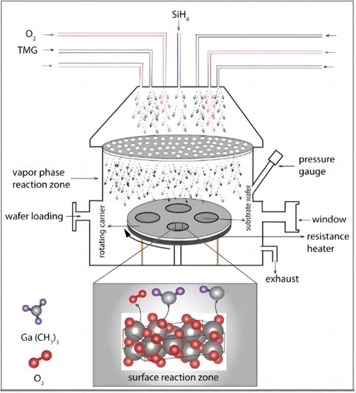
Epitaxy Process Methods
There are several epitaxy methods: liquid phase epitaxy(LPE), hybrid vapor phase epitaxy, solid phase epitaxy, atomic layer deposition, chemical vapor deposition, molecular beam epitaxy, etc. Let's compare two epitaxy processes: CVD and MBE.
Chemical vapor deposition (CVD) Molecular beam epitaxy (MBE)
Chemical process Physical process
Involves a chemical reaction that occurs when a gas precursor meets a heated substrate in a growth chamber or reactor The material to be deposited is heated under vacuum conditions
Precise control of the film growth process Precise control of the thickness and composition of the grown layer
For applications that require high-quality epitaxial layers For applications that require extremely fine epitaxial layers
Most commonly used method More expensive method
| Chemical vapor deposition (CVD) | Molecular beam epitaxy (MBE) |
| Chemical process | Physical process |
| Involves a chemical reaction that occurs when a gas precursor meets a heated substrate in a growth chamber or reactor | The material to be deposited is heated under vacuum conditions |
| Precise control of the thin film growth process | Precise control of the thickness and composition of the grown layer |
| Used in applications requiring high-quality epitaxial layers | Used in applications requiring extremely fine epitaxial layers |
| Most commonly used method | More expensive method |
Chemical vapor deposition (CVD) Molecular beam epitaxy (MBE)
Chemical process Physical process
Involves a chemical reaction that occurs when a gas precursor meets a heated substrate in a growth chamber or reactor The material to be deposited is heated under vacuum conditions
Precise control of the thin film growth process Precise control of the thickness and composition of the grown layer
Used in applications requiring high-quality epitaxial layers Used in applications requiring extremely fine epitaxial layers
Most commonly used method More expensive method
The epitaxy process is critical in semiconductor manufacturing; it optimizes the performance of
semiconductor devices and integrated circuits. It is one of the main processes in semiconductor device manufacturing that affects device quality, characteristics, and electrical performance.


