
- English
- Español
- Português
- русский
- Français
- 日本語
- Deutsch
- tiếng Việt
- Italiano
- Nederlands
- ภาษาไทย
- Polski
- 한국어
- Svenska
- magyar
- Malay
- বাংলা ভাষার
- Dansk
- Suomi
- हिन्दी
- Pilipino
- Türkçe
- Gaeilge
- العربية
- Indonesia
- Norsk
- تمل
- český
- ελληνικά
- український
- Javanese
- فارسی
- தமிழ்
- తెలుగు
- नेपाली
- Burmese
- български
- ລາວ
- Latine
- Қазақша
- Euskal
- Azərbaycan
- Slovenský jazyk
- Македонски
- Lietuvos
- Eesti Keel
- Română
- Slovenski
- मराठी
- Srpski језик

What is the difference between epitaxy and ALD?
2024-08-13
The main difference between epitaxy and atomic layer deposition (ALD) lies in their film growth mechanisms and operating conditions. Epitaxy refers to the process of growing a crystalline thin film on a crystalline substrate with a specific orientation relationship, maintaining the same or similar crystal structure. In contrast, ALD is a deposition technique that involves exposing a substrate to different chemical precursors in sequence to form a thin film one atomic layer at a time.
Differences:
Epitaxy refers to the growth of a single crystalline thin film on a substrate, maintaining a specific crystal orientation. Epitaxy is often used to create semiconductor layers with precisely controlled crystal structures.
ALD is a method of depositing thin films through an ordered, self-limiting chemical reaction between gaseous precursors. It focuses on achieving precise thickness control and excellent consistency, regardless of the substrate's crystal structure.
Detailed description:
Film growth mechanism:
Epitaxy: During epitaxial growth, the film grows in such a way that its crystal lattice is aligned with that of the substrate. This alignment is critical to electronic properties and is typically achieved through processes such as molecular beam epitaxy (MBE) or chemical vapor deposition (CVD) under specific conditions that promote orderly film growth.
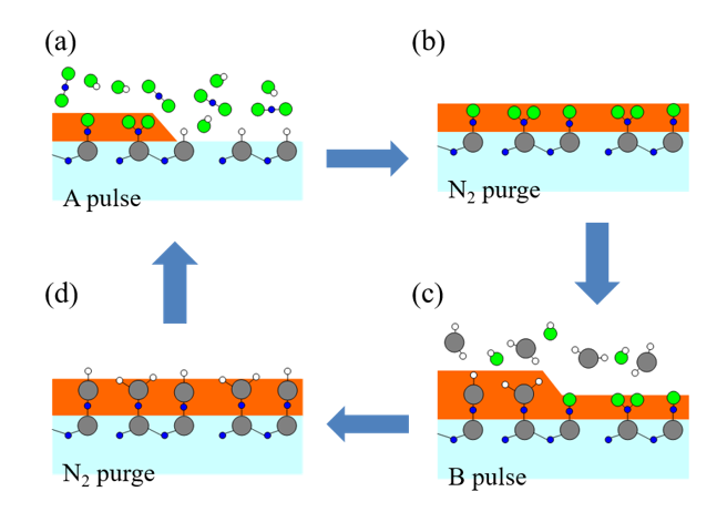
ALD:ALD uses a different principle to grow thin films through a series of self-limiting surface reactions. Each cycle requires exposing the substrate to a precursor gas, which adsorbs onto the substrate surface and reacts to form a monolayer. The chamber is then purged and a second precursor is introduced to react with the first monolayer to form a complete layer. This cycle repeats until the desired film thickness is achieved.
Control and Precision:
Epitaxy: While epitaxy provides good control over crystal structure, it may not provide the same level of thickness control as ALD, especially at the atomic scale. Epitaxy focuses on maintaining the integrity and orientation of the crystal.
ALD:ALD excels at precisely controlling film thickness, down to the atomic level. This precision is critical in applications such as semiconductor manufacturing and nanotechnology that require extremely thin, uniform films.
Applications and Flexibility:
Epitaxy:Epitaxy is commonly used in semiconductor manufacturing because the electronic properties of a film are largely dependent on its crystal structure. Epitaxy is less flexible in terms of the materials that can be deposited and the types of substrates that can be used.
ALD: ALD is more versatile, capable of depositing a wide range of materials and conforming to complex, high-aspect ratio structures. It can be used in a variety of fields including electronics, optics, and energy applications, where conformal coatings and precise thickness control are critical.
In summary, while both epitaxy and ALD are used to deposit thin films, they serve different purposes and work on different principles. Epitaxy is more focused on maintaining crystal structure and orientation, while ALD focuses on precise atomic-level thickness control and excellent conformality.
Previous:What is CVD TAC Coating? - Veteksemi


