- English
- Español
- Português
- русский
- Français
- 日本語
- Deutsch
- tiếng Việt
- Italiano
- Nederlands
- ภาษาไทย
- Polski
- 한국어
- Svenska
- magyar
- Malay
- বাংলা ভাষার
- Dansk
- Suomi
- हिन्दी
- Pilipino
- Türkçe
- Gaeilge
- العربية
- Indonesia
- Norsk
- تمل
- český
- ελληνικά
- український
- Javanese
- فارسی
- தமிழ்
- తెలుగు
- नेपाली
- Burmese
- български
- ລາວ
- Latine
- Қазақша
- Euskal
- Azərbaycan
- Slovenský jazyk
- Македонски
- Lietuvos
- Eesti Keel
- Română
- Slovenski
- मराठी
- Srpski језик
Why does 3C-SiC stand out among many SiC polymorphs? - VeTek Semiconductor
2024-10-16
The background of SiC
Silicon carbide (SiC) is an important high-end precision semiconductor material. Due to its good high temperature resistance, corrosion resistance, wear resistance, high temperature mechanical properties, oxidation resistance and other characteristics, it has broad application prospects in high-tech fields such as semiconductors, nuclear energy, national defense and space technology.
So far, more than 200 SiC crystal structures have been confirmed, the main types are hexagonal (2H-SiC, 4H-SiC, 6H-SiC) and cubic 3C-SiC. Among them, the equiaxed structural characteristics of 3C-SiC determine that this type of powder has better natural sphericity and dense stacking characteristics than α-SiC, so it has better performance in precision grinding, ceramic products and other fields. At present, various reasons have led to the failure of the excellent performance of 3C-SiC new materials to achieve large-scale industrial applications.

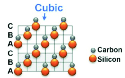
Among many SiC polytypes, 3C-SiC is the only cubic polytype, also known as β-SiC. In this crystal structure, Si and C atoms exist in the lattice in a one-to-one ratio, and each atom is surrounded by four heterogeneous atoms, forming a tetrahedral structural unit with strong covalent bonds. The structural feature of 3C-SiC is that the Si-C diatomic layers are repeatedly arranged in the order of ABC-ABC-…, and each unit cell contains three such diatomic layers, which is called C3 representation; the crystal structure of 3C-SiC is shown in the figure below:
Currently, silicon (Si) is the most commonly used semiconductor material for power devices. However, due to the performance of Si, silicon-based power devices are limited. Compared with 4H-SiC and 6H-SiC, 3C-SiC has the highest room temperature theoretical electron mobility (1000 cm·V-1·S-1), and has more advantages in MOS device applications. At the same time, 3C-SiC also has excellent properties such as high breakdown voltage, good thermal conductivity, high hardness, wide bandgap, high temperature resistance, and radiation resistance. Therefore, it has great potential in electronics, optoelectronics, sensors, and applications under extreme conditions, promoting the development and innovation of related technologies, and showing wide application potential in many fields:
First: Especially in high voltage, high frequency and high temperature environments, the high breakdown voltage and high electron mobility of 3C-SiC make it an ideal choice for manufacturing power devices such as MOSFET.
Second: The application of 3C-SiC in nanoelectronics and microelectromechanical systems (MEMS) benefits from its compatibility with silicon technology, allowing the manufacture of nanoscale structures such as nanoelectronics and nanoelectromechanical devices.
Third: As a wide bandgap semiconductor material, 3C-SiC is suitable for the manufacture of blue light-emitting diodes (LEDs). Its application in lighting, display technology and lasers has attracted attention due to its high luminous efficiency and easy doping[9]. Fourth: At the same time, 3C-SiC is used to manufacture position-sensitive detectors, especially laser point position-sensitive detectors based on the lateral photovoltaic effect, which show high sensitivity under zero bias conditions and are suitable for precision positioning.
Preparation method of 3C SiC heteroepitaxy
The main growth methods of 3C-SiC heteroepitaxial include chemical vapor deposition (CVD), sublimation epitaxy (SE), liquid phase epitaxy (LPE), molecular beam epitaxy (MBE), magnetron sputtering, etc. CVD is the preferred method for 3C-SiC epitaxy due to its controllability and adaptability (such as temperature, gas flow, chamber pressure and reaction time, which can optimize the quality of the epitaxial layer).

Chemical vapor deposition (CVD): A compound gas containing Si and C elements is passed into the reaction chamber, heated and decomposed at high temperature, and then Si atoms and C atoms are precipitated onto the Si substrate, or 6H-SiC, 15R-SiC, 4H-SiC substrate. The temperature of this reaction is usually between 1300-1500℃. Common Si sources are SiH4, TCS, MTS, etc., and C sources are mainly C2H4, C3H8, etc., and H2 is used as the carrier gas.
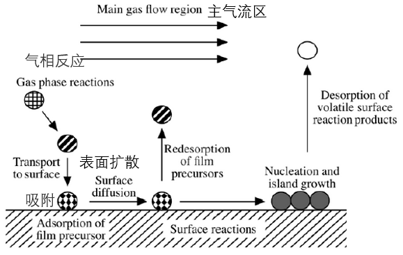
The growth process mainly includes the following steps:
1. The gas phase reaction source is transported in the main gas flow toward the deposition zone.
2. The gas phase reaction occurs in the boundary layer to generate thin film precursors and byproducts.
3. The precipitation, adsorption and cracking process of the precursor.
4. The adsorbed atoms migrate and reconstruct on the substrate surface.
5. The adsorbed atoms nucleate and grow on the substrate surface.
6. The mass transport of the waste gas after the reaction into the main gas flow zone and is taken out of the reaction chamber.
Through continuous technological progress and in-depth mechanism research, 3C-SiC heteroepitaxial technology is expected to play a more important role in the semiconductor industry and promote the development of high-efficiency electronic devices. For example, the rapid growth of high-quality thick film 3C-SiC is the key to meeting the needs of high-voltage devices. Further research is needed to overcome the balance between growth rate and material uniformity; combined with the application of 3C-SiC in heterogeneous structures such as SiC/GaN, explore its potential applications in new devices such as power electronics, optoelectronic integration and quantum information processing.
Vetek Semiconductor provides 3C SiC coating on different products, such as high-purity graphite and high-purity silicon carbide. With more than 20 years of R&D experience, our company selects highly matching materials, such as Si Epi susceptor, SiC epitaxial susceptor, GaN on Si epi susceptor, etc., which play an important role in the epitaxial layer production process.
If you have any inquiries or need additional details, please don't hesitate to get in touch with us.
Mob/WhatsAPP: +86-180 6922 0752
Email: anny@veteksemi.com


