
- English
- Español
- Português
- русский
- Français
- 日本語
- Deutsch
- tiếng Việt
- Italiano
- Nederlands
- ภาษาไทย
- Polski
- 한국어
- Svenska
- magyar
- Malay
- বাংলা ভাষার
- Dansk
- Suomi
- हिन्दी
- Pilipino
- Türkçe
- Gaeilge
- العربية
- Indonesia
- Norsk
- تمل
- český
- ελληνικά
- український
- Javanese
- فارسی
- தமிழ்
- తెలుగు
- नेपाली
- Burmese
- български
- ລາວ
- Latine
- Қазақша
- Euskal
- Azərbaycan
- Slovenský jazyk
- Македонски
- Lietuvos
- Eesti Keel
- Română
- Slovenski
- मराठी
- Srpski језик
Diamond - the future star of semiconductors
2024-10-15
With the rapid development of science and technology and the growing global demand for high-performance and high-efficiency semiconductor devices, semiconductor substrate materials, as a key technical link in the semiconductor industry chain, are becoming increasingly important. Among them, diamond, as a potential fourth-generation "ultimate semiconductor" material, is gradually becoming a research hotspot and a new market favorite in the field of semiconductor substrate materials due to its excellent physical and chemical properties.
Properties of diamond
Diamond is a typical atomic crystal and covalent bond crystal. The crystal structure is shown in Figure 1(a). It consists of the middle carbon atom bonded to the other three carbon atoms in the form of a covalent bond. Figure 1(b) is the unit cell structure, which reflects the microscopic periodicity and structural symmetry of diamond.
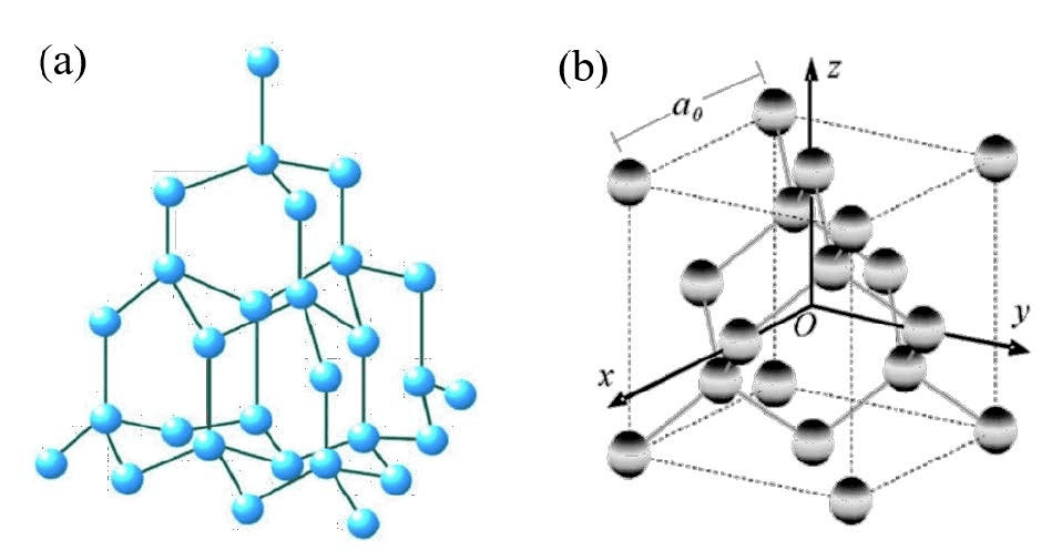
Figure 1 Diamond (a) crystal structure; (b) unit cell structure
Diamond is the hardest material in the world, with unique physical and chemical properties, and excellent properties in mechanics, electricity and optics, as shown in Figure 2: Diamond has ultra-high hardness and wear resistance, suitable for cutting materials and indenters, etc., and is well used in abrasive tools; (2) Diamond has the highest thermal conductivity (2200W/(m·K)) among natural substances known to date, which is 4 times greater than silicon carbide (SiC), 13 times greater than silicon (Si), 43 times greater than gallium arsenide (GaAs), and 4 to 5 times greater than copper and silver, and is used in high-power devices. It has excellent properties such as low thermal expansion coefficient (0.8×10⁻⁶-1.5×10⁻⁶K-1) and high elastic modulus. It is an excellent electronic packaging material with good prospects.
The hole mobility is 4500 cm2·V-1·s-1, and the electron mobility is 3800 cm2·V-1·s-1, which makes it applicable to high-speed switching devices; the breakdown field strength is 13MV/cm, which can be applied to high-voltage devices; the Baliga figure of merit is as high as 24664, which is much higher than other materials (the larger the value, the greater the potential for use in switching devices).
Polycrystalline diamond also has a decorative effect. The diamond coating not only has a flash effect but also has a variety of colors. It is used in the manufacture of high-end watches, decorative coatings for luxury goods, and directly as a fashion product. The strength and hardness of diamond are 6 times and 10 times that of Corning glass, so it is also used in mobile phone displays and camera lenses.
![]()
Figure 2 Properties of diamond and other semiconductor materials
Preparation of diamond
Diamond growth is mainly divided into HTHP method (high temperature and high pressure method) and CVD method (chemical vapor deposition method). The CVD method has become the mainstream method for preparing diamond semiconductor substrates due to its advantages such as high pressure resistance, large radio frequency, low cost, and high temperature resistance. The two growth methods focus on different applications, and they will show a complementary relationship for a long time in the future.
The high temperature and high pressure method (HTHP) is to make a graphite core column by mixing graphite powder, metal catalyst powder and additives in the proportion specified by the raw material formula, and then granulating, static pressing, vacuum reduction, inspection, weighing and other processes. The graphite core column is then assembled with the composite block, auxiliary parts and other sealed pressure transmission media to form a synthetic block that can be used to synthesize diamond single crystals. After that, it is placed in a six-sided top press for heating and pressurization and kept constant for a long time. After the crystal growth is completed, the heat is stopped and the pressure is released, and the sealed pressure transmission medium is removed to obtain the synthetic column, which is then purified and sorted to obtain diamond single crystals.
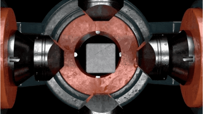
Figure 3 Structure diagram of six-sided top press
Due to the use of metal catalysts, diamond particles prepared by the industrial HTHP method often contain certain impurities and defects, and due to the addition of nitrogen, they usually have a yellow hue. After the technology upgrade, the high temperature and high pressure preparation of diamonds can use the temperature gradient method to produce large-particle high-quality diamond single crystals, realizing the transformation of diamond industrial abrasive grade to gem grade.
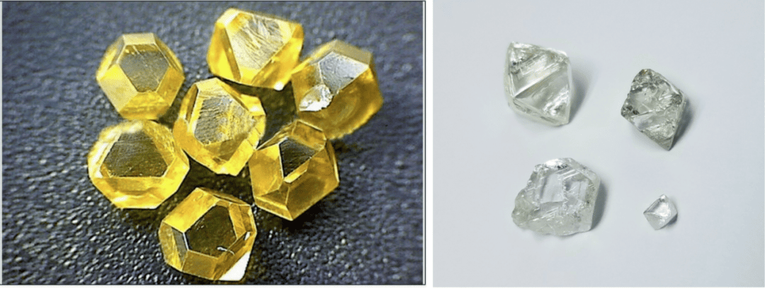
Figure 4 Diamond morphology
Chemical vapor deposition (CVD) is the most popular method for synthesizing diamond films. The main methods include hot filament chemical vapor deposition (HFCVD) and microwave plasma chemical vapor deposition (MPCVD).
(1) Hot filament chemical vapor deposition
The basic principle of HFCVD is to collide the reaction gas with a high-temperature metal wire in a vacuum chamber to generate a variety of highly active "uncharged" groups. The generated carbon atoms are deposited on the substrate material to form nanodiamonds. The equipment is simple to operate, has low growth cost, is widely used, and is easy to achieve industrial production. Due to the low thermal decomposition efficiency and the serious metal atom contamination from the filament and electrode, HFCVD is usually only used to prepare polycrystalline diamond films containing a large amount of sp2 phase carbon impurities at the grain boundary, so it is generally gray-black.
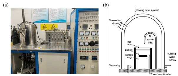
Figure 5 (a) HFCVD equipment diagram, (b) vacuum chamber structure diagram
(2) Microwave plasma chemical vapor deposition
MPCVD method uses magnetron or solid-state source to generate microwaves of specific frequency, which are fed into the reaction chamber through waveguide, and form stable standing waves above the substrate according to the special geometric dimensions of the reaction chamber.
The highly focused electromagnetic field breaks down the reaction gases methane and hydrogen here to form a stable plasma ball. The electron-rich, ion-rich, and active atomic groups will nucleate and grow on the substrate at the appropriate temperature and pressure, causing homoepitaxial growth slowly. Compared with HFCVD, it avoids the contamination of the diamond film caused by hot metal wire evaporation and increases the purity of the nanodiamond film. More reaction gases can be used in the process than HFCVD, and the deposited diamond single crystals are purer than natural diamonds. Therefore, optical-grade diamond polycrystalline windows, electronic-grade diamond single crystals, etc. can be prepared.
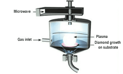
Figure 6 Internal structure of MPCVD
Development and dilemma of diamond
Since the first artificial diamond was successfully developed in 1963, after more than 60 years of development, my country has become the country with the largest output of artificial diamond in the world, accounting for more than 90% of the world. However, China's diamonds are mainly concentrated in the low-end and medium-end application markets, such as abrasive grinding, optics, sewage treatment and other fields. The development of domestic diamonds is large but not strong, and it is at a disadvantage in many fields such as high-end equipment and electronic-grade materials.
In terms of academic achievements in the field of CVD diamonds, the research in the United States, Japan and Europe is in a leading position, and there are relatively few original research in my country. With the support of the key research and development of the "13th Five-Year Plan", domestic spliced epitaxial large-size diamond single crystals have leaped to the world's first-class position. In terms of heterogeneous epitaxial single crystals, there is still a large gap in size and quality, which may be surpassed in the "14th Five-Year Plan".
Researchers from all over the world have conducted in-depth research on the growth, doping, and device assembly of diamonds in order to realize the application of diamonds in optoelectronic devices and meet people's expectations for diamonds as a multifunctional material. However, the band gap of diamond is as high as 5.4 eV. Its p-type conductivity can be achieved by boron doping, but it is very difficult to obtain n-type conductivity. Researchers from various countries have doped impurities such as nitrogen, phosphorus, and sulfur into single crystal or polycrystalline diamond in the form of replacing carbon atoms in the lattice. However, due to the deep donor energy level or difficulty in ionization of the impurities, good n-type conductivity has not been obtained, which greatly limits the research and application of diamond-based electronic devices.
At the same time, large-area single crystal diamond is difficult to prepare in large quantities like single crystal silicon wafers, which is another difficulty in the development of diamond-based semiconductor devices. The above two problems show that the existing semiconductor doping and device development theory is difficult to solve the problems of diamond n-type doping and device assembly. It is necessary to seek other doping methods and dopants, or even develop new doping and device development principles.
Excessively high prices also limit the development of diamonds. Compared with the price of silicon, the price of silicon carbide is 30-40 times that of silicon, the price of gallium nitride is 650-1300 times that of silicon, and the price of synthetic diamond materials is roughly 10,000 times that of silicon. Too high a price limits the development and application of diamonds. How to reduce costs is a breakthrough point to break the development dilemma.
Outlook
Although diamond semiconductors are currently facing difficulties in development, they are still considered to be the most promising material for preparing the next generation of high-power, high-frequency, high-temperature and low-power loss electronic devices. Currently, the hottest semiconductors are occupied by silicon carbide. Silicon carbide has the structure of diamond, but half of its atoms are carbon. Therefore, it can be regarded as half a diamond. Silicon carbide should be a transitional product from the silicon crystal era to the diamond semiconductor era.
The phrase "Diamonds are forever, and one diamond lasts forever" has made the name of De Beers famous to this day. For diamond semiconductors, creating another kind of glory may require permanent and continuous exploration.
VeTek Semiconductor is a professional Chinese manufacturer of Tantalum Carbide Coating, Silicon Carbide Coating, GaN products, Special Graphite, Silicon Carbide Ceramics and Other Semiconductor Ceramics. VeTek Semiconductor is committed to providing advanced solutions for various Coating products for the semiconductor industry.
If you have any inquiries or need additional details, please don't hesitate to get in touch with us.
Mob/WhatsAPP: +86-180 6922 0752
Email: anny@veteksemi.com


