- English
- Español
- Português
- русский
- Français
- 日本語
- Deutsch
- tiếng Việt
- Italiano
- Nederlands
- ภาษาไทย
- Polski
- 한국어
- Svenska
- magyar
- Malay
- বাংলা ভাষার
- Dansk
- Suomi
- हिन्दी
- Pilipino
- Türkçe
- Gaeilge
- العربية
- Indonesia
- Norsk
- تمل
- český
- ελληνικά
- український
- Javanese
- فارسی
- தமிழ்
- తెలుగు
- नेपाली
- Burmese
- български
- ລາວ
- Latine
- Қазақша
- Euskal
- Azərbaycan
- Slovenský jazyk
- Македонски
- Lietuvos
- Eesti Keel
- Română
- Slovenski
- मराठी
- Srpski језик
How Porous Graphite Enhances Silicon Carbide Crystal Growth?
2025-01-09
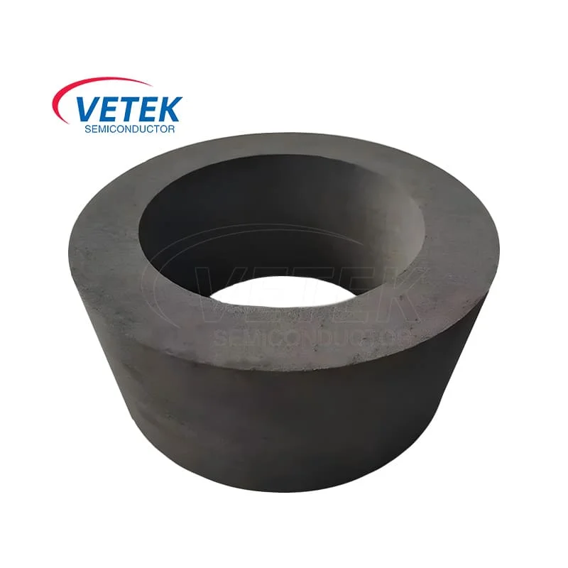
Porous graphite is transforming silicon carbide (SiC) crystal growth by addressing critical limitations in the Physical Vapor Transport (PVT) method. Its porous structure enhances gas flow and ensures temperature homogeneity, which are essential for producing high-quality SiC crystals. This material also reduces stress and improves heat dissipation, minimizing defects and impurities. These advancements represent a breakthrough in semiconductor technology, enabling the development of efficient electronic devices. By optimizing the PVT process, porous graphite has become a cornerstone for achieving superior SiC crystal purity and performance.
Ⅰ. Key Takeaways
● Porous graphite helps SiC crystals grow better by improving gas flow. It also keeps the temperature even, creating higher quality crystals.
● The PVT method uses porous graphite to lower defects and impurities. This makes it very important for making semiconductors efficiently.
● New improvements in porous graphite, like adjustable pore sizes and high porosity, make the PVT process better. This boosts the performance of modern power devices.
● Porous graphite is strong, reusable, and supports eco-friendly semiconductor production. Recycling it saves 30% of energy use.
Ⅱ. The Role of Silicon Carbide in Semiconductor Technology
The Physical Vapor Transport (PVT) Method for SiC Growth
The PVT method is the most widely used technique for growing high-quality SiC crystals. This process involves:
● Heating a crucible containing polycrystalline SiC to over 2000°C, causing sublimation.
● Transporting the vaporized SiC to a cooler area where a seed crystal is placed.
● Solidifying the vapor on the seed crystal, forming crystalline layers.
The process occurs in a sealed graphite crucible, which ensures a controlled environment. Porous graphite plays a critical role in optimizing this method by enhancing gas flow and thermal management, leading to improved crystal quality.
Challenges in Achieving High-Quality SiC Crystals
Despite its advantages, producing defect-free SiC crystals remains challenging. Issues such as thermal stress, impurity incorporation, and non-uniform growth often arise during the PVT process. These defects can compromise the performance of SiC-based devices. Innovations in materials like porous graphite are addressing these challenges by improving temperature control and reducing impurities, paving the way for higher-quality crystals.
Ⅲ. Unique Properties of Porous Graphite
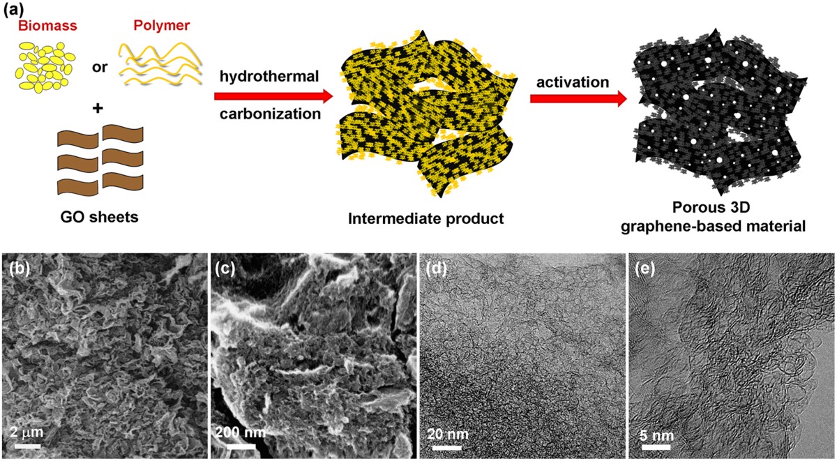
Porous graphite exhibits a range of properties that make it an ideal material for silicon carbide crystal growth. Its unique characteristics enhance the efficiency and quality of the Physical Vapor Transport (PVT) process, addressing challenges like thermal stress and impurity incorporation.
Porosity and Enhanced Gas Flow
The porosity of porous graphite plays a pivotal role in improving gas flow during the PVT process. Its customizable pore sizes allow precise control over gas distribution, ensuring uniform vapor transport across the growth chamber. This uniformity minimizes the risk of non-uniform crystal growth, which can lead to defects. Additionally, the lightweight nature of porous graphite reduces the overall stress on the system, further contributing to the stability of the crystal growth environment.
Thermal Conductivity for Temperature Control
High thermal conductivity is one of the defining features of porous graphite. This property ensures effective thermal management, which is critical for maintaining stable temperature gradients during silicon carbide crystal growth. Consistent temperature control prevents thermal stress, a common issue that can lead to cracks or other structural defects in the crystals. For high-power applications, such as those in electric vehicles and renewable energy systems, this level of precision is indispensable.
Mechanical Stability and Impurity Suppression
Porous graphite demonstrates excellent mechanical stability, even under extreme conditions. Its ability to withstand high temperatures with minimal thermal expansion ensures that the material maintains its structural integrity throughout the PVT process. Furthermore, its corrosion resistance helps suppress impurities, which could otherwise compromise the quality of the silicon carbide crystals. These attributes make porous graphite a reliable choice for producing high-purity crystals in demanding semiconductor applications.
Ⅳ. How Porous Graphite Optimizes the PVT Process
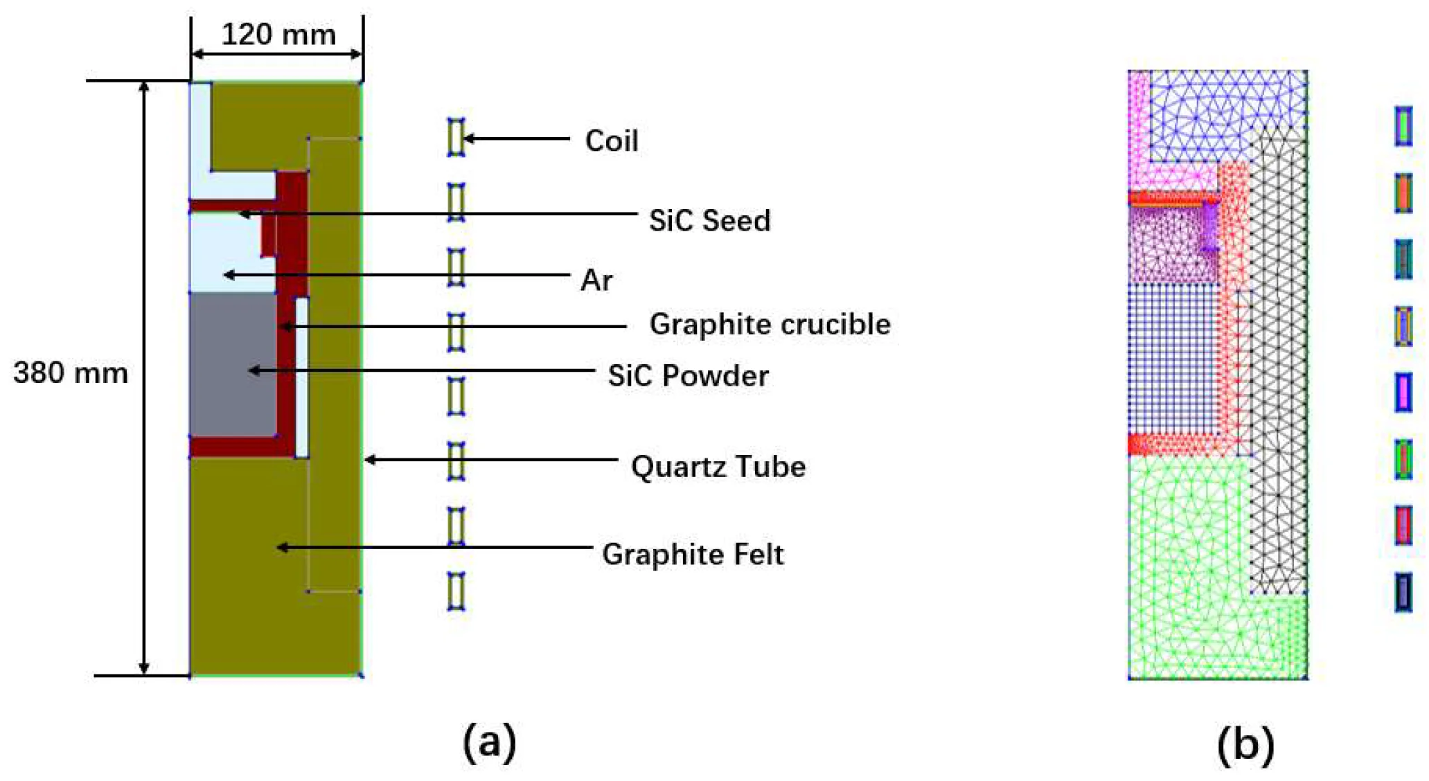
Improved Mass Transfer and Vapor Transport
Porous graphite significantly enhances mass transfer and vapor transport during the Physical Vapor Transport (PVT) process. Its porous structure improves purification ability, which is essential for efficient mass transfer. By balancing gas phase components and isolating impurities, it ensures a more consistent growth environment. This material also adjusts local temperatures, creating optimal conditions for vapor transport. These improvements reduce the impact of recrystallization, stabilizing the growth process and leading to higher-quality silicon carbide crystals.
Key benefits of porous graphite in mass transfer and vapor transport include:
● Enhanced purification ability for effective mass transfer.
● Stabilized gas phase components, reducing impurity incorporation.
● Improved consistency in vapor transport, minimizing recrystallization effects.
Uniform Thermal Gradients for Crystal Stability
Uniform thermal gradients play a critical role in stabilizing silicon carbide crystals during growth. Research has shown that optimized thermal fields create a nearly flat and slightly convex growth interface. This configuration minimizes structural defects and ensures consistent crystal quality. For instance, a study demonstrated that maintaining uniform thermal gradients enabled the production of a high-quality 150 mm single crystal with minimal defects. Porous graphite contributes to this stability by promoting even heat distribution, which prevents thermal stress and supports the formation of defect-free crystals.
Reduction of Defects and Impurities in SiC Crystals
Porous graphite reduces defects and impurities in silicon carbide crystals, making it a game-changer for the PVT process. Furnaces utilizing porous graphite have achieved a micro-pipe density (MPD) of 1-2 EA/cm², compared to 6-7 EA/cm² in traditional systems. This sixfold reduction highlights its effectiveness in producing higher-quality crystals. Additionally, substrates grown with porous graphite exhibit significantly lower etch pit density (EPD), further confirming its role in impurity suppression.
Aspect
Improvement Description
Temperature Uniformity
Porous graphite enhances overall temperature and uniformity, promoting better sublimation of raw materials.
Mass Transfer
It reduces mass transfer rate fluctuations, stabilizing the growth process.
C/Si Ratio
Increases the carbon to silicon ratio, reducing phase changes during growth.
Recrystallization
Increases the carbon to silicon ratio, reducing phase changes during growth.
Growth Rate
Slows down growth rate but maintains a convex interface for better quality.
These advancements underscore the transformative impact of porous graphite on the PVT process, enabling the production of defect-free silicon carbide crystals for next-generation semiconductor applications.
Ⅴ. Recent Innovations in Porous Graphite Materials
Advances in Porosity Control and Customization
Recent advancements in porosity control have significantly improved the performance of porous graphite in silicon carbide crystal growth. Researchers have developed methods to achieve porosity levels of up to 65%, setting a new international standard. This high porosity allows for enhanced gas flow and better temperature regulation during the Physical Vapor Transport (PVT) process. Evenly distributed voids within the material ensure consistent vapor transport, reducing the likelihood of defects in the resulting crystals.
Customization of pore sizes has also become more precise. Manufacturers can now tailor the pore structure to meet specific requirements, optimizing the material for different crystal growth conditions. This level of control minimizes thermal stress and impurity incorporation, leading to higher-quality silicon carbide crystals. These innovations underscore the critical role of porous graphite in advancing semiconductor technology.
New Manufacturing Techniques for Scalability
To meet the growing demand for porous graphite, new manufacturing techniques have emerged that enhance scalability without compromising quality. Additive manufacturing, such as 3D printing, is being explored to create complex geometries and precisely control pore sizes. This approach enables the production of highly customized components that align with specific PVT process requirements.
Other breakthroughs include improvements in batch stability and material strength. Modern techniques now allow for the creation of ultra-thin walls as small as 1 mm, while maintaining high mechanical stability. The table below highlights key features of these advancements:
Feature
Description
Porosity
Up to 65% (international leading)
Voids distribution
Evenly distributed
Batch stability
High batch stability
Strength
High strength, can achieve ≤1mm ultra-thin walls
Processability
Leading in the world
These innovations ensure that porous graphite remains a scalable and reliable material for semiconductor manufacturing.
Implications for 4H-SiC Crystal Growth
The latest developments in porous graphite have profound implications for the growth of 4H-SiC crystals. Enhanced gas flow and improved temperature homogeneity contribute to a more stable growth environment. These improvements reduce stress and enhance heat dissipation, resulting in high-quality single crystals with fewer defects.
Key benefits include:
● Enhanced purification ability, which minimizes trace impurities during crystal growth.
● Improved mass transfer efficiency, ensuring a consistent transfer rate
● Reduction of microtubules and other defects through optimized thermal fields.
Aspect
Description
Purification Ability
Porous graphite enhances purification, reducing trace impurities during crystal growth.
Mass Transfer Efficiency
The new process improves mass transfer efficiency, maintaining a consistent transfer rate.
Defect Reduction
Reduces the risk of microtubules and associated crystal defects through optimized thermal fields.
These advancements position porous graphite as a cornerstone material for producing defect-free 4H-SiC crystals, which are essential for next-generation semiconductor devices.
Ⅵ. Future Applications of Porous Graphite in Semiconductors
Expanding Use in Next-Generation Power Devices
Porous graphite is becoming a vital material in next-generation power devices due to its exceptional properties. Its high thermal conductivity ensures efficient heat dissipation, which is critical for devices operating under high power loads. The lightweight nature of porous graphite reduces the overall weight of components, making it ideal for compact and portable applications. Additionally, its customizable microstructure allows manufacturers to tailor the material for specific thermal and mechanical requirements.
Other advantages include excellent corrosion resistance and the ability to manage thermal gradients effectively. These features promote uniform temperature distribution, which enhances the reliability and longevity of power devices. Applications such as electric vehicle inverters, renewable energy systems, and high-frequency power converters benefit significantly from these properties. By addressing the thermal and structural challenges of modern power electronics, porous graphite is paving the way for more efficient and durable devices.
Sustainability and Scalability in Semiconductor Manufacturing
Porous graphite contributes to sustainability in semiconductor manufacturing through its durability and reusability. Its robust structure allows for multiple uses, reducing waste and operational costs. Innovations in recycling techniques further enhance its sustainability. Advanced methods recover and purify used porous graphite, cutting energy consumption by 30% compared to producing new material.
These advancements make porous graphite a cost-effective and environmentally friendly choice for semiconductor production. Its scalability is also noteworthy. Manufacturers can now produce porous graphite in large quantities without compromising quality, ensuring a steady supply for the growing semiconductor industry. This combination of sustainability and scalability positions porous graphite as a cornerstone material for future semiconductor technologies.
Potential for Broader Applications Beyond SiC Crystals
The versatility of porous graphite extends beyond silicon carbide crystal growth. In water treatment and filtration, it effectively removes contaminants and impurities. Its ability to selectively adsorb gases makes it valuable for gas separation and storage. Electrochemical applications, such as batteries, fuel cells, and capacitors, also benefit from its unique properties.
Porous graphite serves as a support material in catalysis, enhancing the efficiency of chemical reactions. Its thermal management capabilities make it suitable for heat exchangers and cooling systems. In the medical and pharmaceutical fields, its biocompatibility enables its use in drug delivery systems and biosensors. These diverse applications highlight the potential of porous graphite to revolutionize multiple industries.
Porous graphite has emerged as a transformative material in the production of high-quality silicon carbide crystals. Its ability to enhance gas flow and manage thermal gradients addresses critical challenges in the Physical Vapor Transport process. Recent studies highlight its potential to reduce thermal resistance by up to 50%, significantly improving device performance and lifespan.
Studies reveal that graphite-based TIMs can reduce thermal resistance by up to 50% compared to conventional materials, significantly enhancing device performance and lifespan.
Ongoing advancements in graphite material science are reshaping its role in semiconductor manufacturing. Researchers are focusing on developing high-purity, high-strength graphite to meet the demands of modern semiconductor technologies. Emerging forms like graphene, with exceptional thermal and electrical properties, are also gaining attention for next-generation devices.
As innovations continue, porous graphite will remain a cornerstone in enabling efficient, sustainable, and scalable semiconductor manufacturing, driving the future of technology.
Ⅶ. FAQ
1. What makes porous graphite essential for SiC crystal growth?
Porous graphite enhances gas flow, improves thermal management, and reduces impurities during the Physical Vapor Transport (PVT) process. These properties ensure uniform crystal growth, minimize defects, and enable the production of high-quality silicon carbide crystals for advanced semiconductor applications.
2. How does porous graphite improve the sustainability of semiconductor manufacturing?
Porous graphite’s durability and reusability reduce waste and operational costs. Recycling techniques recover and purify used material, cutting energy consumption by 30%. These features make it an environmentally friendly and cost-effective choice for semiconductor production.
3. Can porous graphite be customized for specific applications?
Yes, manufacturers can tailor porous graphite’s pore size, porosity, and structure to meet specific requirements. This customization optimizes its performance in various applications, including SiC crystal growth, power devices, and thermal management systems.
4. What industries benefit from porous graphite beyond semiconductors?
Porous graphite supports industries like water treatment, energy storage, and catalysis. Its properties make it valuable for filtration, gas separation, batteries, fuel cells, and heat exchangers. Its versatility extends its impact far beyond semiconductor manufacturing.
5. Are there any limitations to using porous graphite?
Porous graphite’s performance depends on precise manufacturing and material quality. Improper porosity control or contamination can affect its efficiency. However, ongoing innovations in production techniques continue to address these challenges effectively.

