
- English
- Español
- Português
- русский
- Français
- 日本語
- Deutsch
- tiếng Việt
- Italiano
- Nederlands
- ภาษาไทย
- Polski
- 한국어
- Svenska
- magyar
- Malay
- বাংলা ভাষার
- Dansk
- Suomi
- हिन्दी
- Pilipino
- Türkçe
- Gaeilge
- العربية
- Indonesia
- Norsk
- تمل
- český
- ελληνικά
- український
- Javanese
- فارسی
- தமிழ்
- తెలుగు
- नेपाली
- Burmese
- български
- ລາວ
- Latine
- Қазақша
- Euskal
- Azərbaycan
- Slovenský jazyk
- Македонски
- Lietuvos
- Eesti Keel
- Română
- Slovenski
- मराठी
- Srpski језик

Chip Manufacturing: Atomic Layer Deposition (ALD)
2024-08-16
In the semiconductor manufacturing industry, as device size continues to shrink, the deposition technology of thin film materials has posed unprecedented challenges. Atomic Layer Deposition (ALD), as a thin film deposition technology that can achieve precise control at the atomic level, has become an indispensable part of semiconductor manufacturing. This article aims to introduce the process flow and principles of ALD to help understand its important role in advanced chip manufacturing.
1. Detailed explanation of the ALD process flow
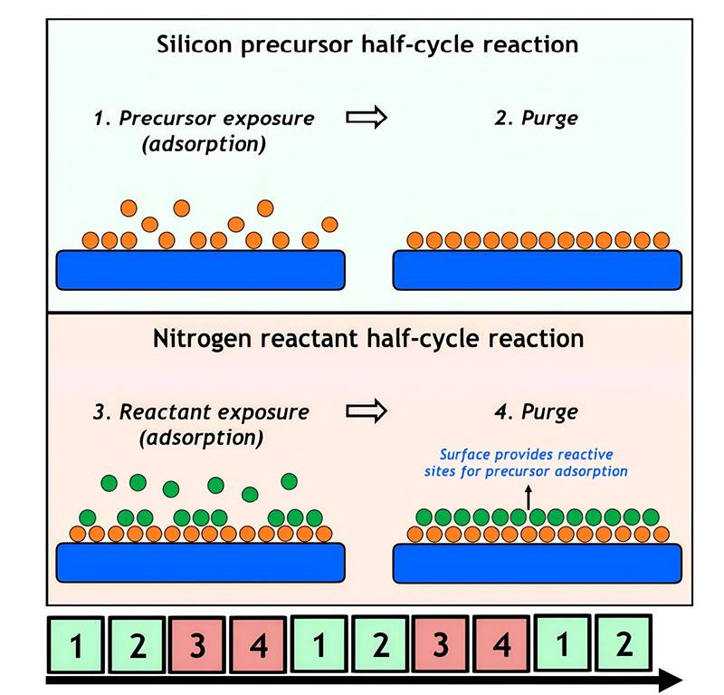
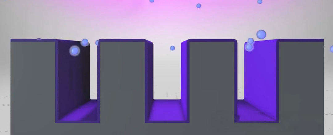
The ALD process follows a strict sequence to ensure that only one atomic layer is added each time deposition, thereby achieving precise control of film thickness. The basic steps are as follows:
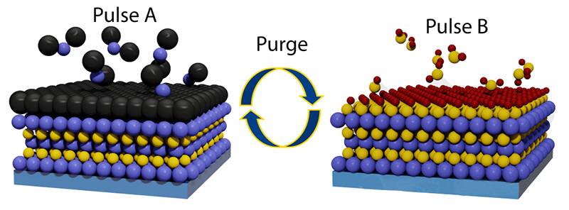
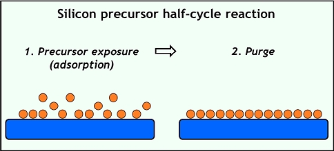
Precursor pulse: The ALD process begins with the introduction of the first precursor into the reaction chamber. This precursor is a gas or vapor containing the chemical elements of the target deposition material that can react with specific active sites on the wafer surface. The precursor molecules are adsorbed on the wafer surface to form a saturated molecular layer.
Inert gas purge: Subsequently, an inert gas (such as nitrogen or argon) is introduced for purge to remove unreacted precursors and byproducts, ensuring that the wafer surface is clean and ready for the next reaction.
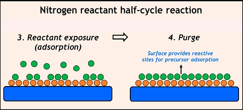
Second precursor pulse: After the purge is completed, the second precursor is introduced to react chemically with the precursor adsorbed in the first step to generate the desired deposit. This reaction is usually self-limiting, that is, once all active sites are occupied by the first precursor, new reactions will no longer occur.
Inert gas purge again: After the reaction is completed, the inert gas is purged again to remove residual reactants and byproducts, restoring the surface to a clean state and preparing for the next cycle.
This series of steps constitutes a complete ALD cycle, and each time a cycle is completed, an atomic layer is added to the wafer surface. By precisely controlling the number of cycles, the desired film thickness can be achieved.
(ALD one cycle step)
2. Process principle analysis
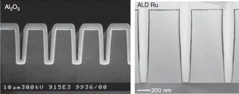
The self-limiting reaction of ALD is its core principle. In each cycle, the precursor molecules can only react with the active sites on the surface. Once these sites are fully occupied, the subsequent precursor molecules cannot be adsorbed, which ensures that only one layer of atoms or molecules is added in each round of deposition. This feature makes ALD have extremely high uniformity and precision when depositing thin films. As shown in the figure below, it can maintain good step coverage even on complex three-dimensional structures.
3. Application of ALD in Semiconductor Manufacturing
ALD is widely used in the semiconductor industry, including but not limited to:
High-k material deposition: used for gate insulation layer of new generation transistors to improve device performance.
Metal gate deposition: such as titanium nitride (TiN) and tantalum nitride (TaN), used to improve the switching speed and efficiency of transistors.
Interconnection barrier layer: prevent metal diffusion and maintain circuit stability and reliability.
Three-dimensional structure filling: such as filling channels in FinFET structures to achieve higher integration.
Atomic layer deposition (ALD) has brought revolutionary changes to the semiconductor manufacturing industry with its extraordinary precision and uniformity. By mastering the process and principles of ALD, engineers are able to build electronic devices with excellent performance at the nanoscale, promoting the continuous advancement of information technology. As technology continues to evolve, ALD will play an even more critical role in the future semiconductor field.
Previous:Do you know about MOCVD Susceptor?


