- English
- Español
- Português
- русский
- Français
- 日本語
- Deutsch
- tiếng Việt
- Italiano
- Nederlands
- ภาษาไทย
- Polski
- 한국어
- Svenska
- magyar
- Malay
- বাংলা ভাষার
- Dansk
- Suomi
- हिन्दी
- Pilipino
- Türkçe
- Gaeilge
- العربية
- Indonesia
- Norsk
- تمل
- český
- ελληνικά
- український
- Javanese
- فارسی
- தமிழ்
- తెలుగు
- नेपाली
- Burmese
- български
- ລາວ
- Latine
- Қазақша
- Euskal
- Azərbaycan
- Slovenský jazyk
- Македонски
- Lietuvos
- Eesti Keel
- Română
- Slovenski
- मराठी
- Srpski језик
What is step-controlled epitaxial growth?
2024-10-25
As one of the core technologies for the preparation of SiC power devices, the quality of epitaxy grown by SiC epitaxial growth technology will directly affect the performance of SiC devices. At present, the most mainstream SiC epitaxial growth technology is chemical vapor deposition (CVD).
There are many stable crystal polytypes of SiC. Therefore, in order to enable the obtained epitaxial growth layer to inherit the specific crystal polytype of the SiC substrate, it is necessary to transfer the three-dimensional atomic arrangement information of the substrate to the epitaxial growth layer, and this requires some special methods. Hiroyuki Matsunami, professor emeritus of Kyoto University, and others proposed such a SiC epitaxial growth technology, which performs chemical vapor deposition (CVD) on the low-index crystal plane of the SiC substrate in a small off-angle direction under appropriate growth conditions. This technical method is also called step-controlled epitaxial growth method.
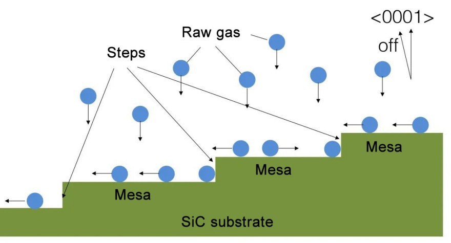
Figure 1 shows how to perform SiC epitaxial growth by step-controlled epitaxial growth method. The surface of a clean and off-angle SiC substrate is formed into layers of steps, and the molecular-level step and table structure is obtained. When the raw material gas is introduced, the raw material is supplied to the surface of the SiC substrate, and the raw material moving on the table is captured by the steps in sequence. When the captured raw material forms an arrangement consistent with the crystal polytype of the SiC substrate at the corresponding position, the epitaxial layer successfully inherits the specific crystal polytype of the SiC substrate.

Figure 1: Epitaxial growth of SiC substrate with an off-angle (0001)
Of course, there may be problems with step-controlled epitaxial growth technology. When the growth conditions do not meet the appropriate conditions, the raw materials will nucleate and generate crystals on the table rather than on the steps, which will lead to the growth of different crystal polytypes, causing the ideal epitaxial layer to fail to grow. If heterogeneous polytypes appear in the epitaxial layer, the semiconductor device may be left with fatal defects. Therefore, in the step-controlled epitaxial growth technology, the degree of deflection must be designed to make the step width reach a reasonable size. At the same time, the concentration of Si raw materials and C raw materials in the raw material gas, the growth temperature and other conditions must also meet the conditions for the priority formation of crystals on the steps. At present, the surface of the main 4H-type SiC substrate on the market presents a 4° deflection angle (0001) surface, which can meet both the requirements of step-controlled epitaxial growth technology and increasing the number of wafers obtained from the boule.
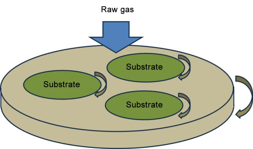
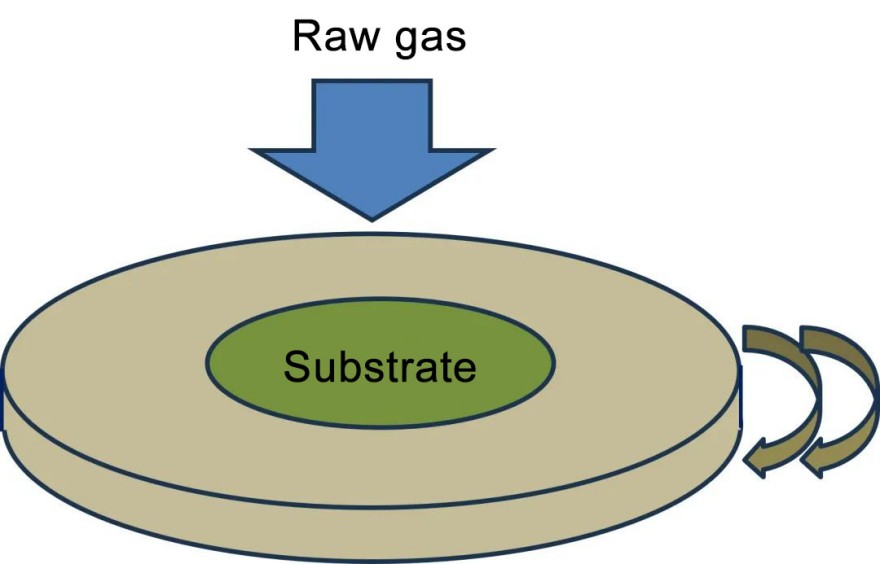
High-purity hydrogen is used as a carrier in the chemical vapor deposition method for SiC epitaxial growth, and Si raw materials such as SiH4 and C raw materials such as C3H8 are input to the surface of the SiC substrate whose substrate temperature is always maintained at 1500-1600℃. At a temperature of 1500-1600°C, if the temperature of the inner wall of the equipment is not high enough, the supply efficiency of the raw materials will not be improved, so it is necessary to use a hot wall reactor. There are many types of SiC epitaxial growth equipment, including vertical, horizontal, multi-wafer and single-wafer types. Figures 2, 3 and 4 show the gas flow and substrate configuration of the reactor part of three types of SiC epitaxial growth equipment.

Figure 2 Multi-chip rotation and revolution

Figure 3 Multi-chip revolution

Figure 4 Single chip
There are several key points to consider in order to achieve mass production of SiC epitaxial substrates: uniformity of epitaxial layer thickness, uniformity of doping concentration, dust, yield, frequency of component replacement, and convenience of maintenance. Among them, the uniformity of doping concentration will directly affect the voltage resistance distribution of the device, so the uniformity of the wafer surface, batch and batch is very high. In addition, the reaction products attached to the components in the reactor and the exhaust system during the growth process will become a dust source, and how to conveniently remove these dusts is also an important research direction.
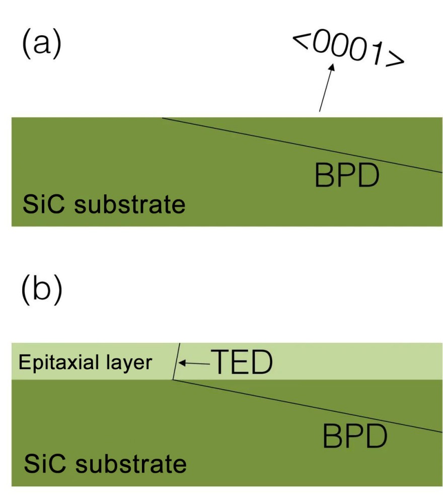
After SiC epitaxial growth, a high-purity SiC single crystal layer that can be used to manufacture power devices is obtained. In addition, through epitaxial growth, the basal plane dislocation (BPD) existing in the substrate can also be converted into a threading edge dislocation (TED) at the substrate/drift layer interface (see Figure 5). When a bipolar current flows through, the BPD will undergo stacking fault expansion, resulting in degradation of device characteristics such as increased on-resistance. However, after the BPD is converted to TED, the electrical characteristics of the device will not be affected. Epitaxial growth can significantly reduce the device degradation caused by bipolar current.

Figure 5: BPD of SiC substrate before and after epitaxial growth and TED cross section after conversion
In the epitaxial growth of SiC, a buffer layer is often inserted between the drift layer and the substrate. The buffer layer with high concentration of n-type doping can promote the recombination of minority carriers. In addition, the buffer layer also has the function of basal plane dislocation (BPD) conversion, which has a considerable impact on the cost and is a very important device manufacturing technology.


