- English
- Español
- Português
- русский
- Français
- 日本語
- Deutsch
- tiếng Việt
- Italiano
- Nederlands
- ภาษาไทย
- Polski
- 한국어
- Svenska
- magyar
- Malay
- বাংলা ভাষার
- Dansk
- Suomi
- हिन्दी
- Pilipino
- Türkçe
- Gaeilge
- العربية
- Indonesia
- Norsk
- تمل
- český
- ελληνικά
- український
- Javanese
- فارسی
- தமிழ்
- తెలుగు
- नेपाली
- Burmese
- български
- ລາວ
- Latine
- Қазақша
- Euskal
- Azərbaycan
- Slovenský jazyk
- Македонски
- Lietuvos
- Eesti Keel
- Română
- Slovenski
- मराठी
- Srpski језик
The Problems in the Etching Process
2024-10-24
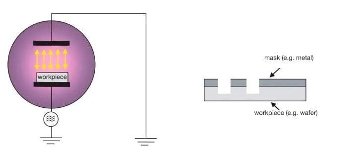
Etching technology is one of the key steps in the semiconductor manufacturing process, which is used to remove specific materials from the wafer to form a circuit pattern. However, during the dry etching process, engineers often encounter problems such as loading effect, micro-groove effect and charging effect, which directly affect the quality and performance of the final product.
Ⅰ Loading Effect
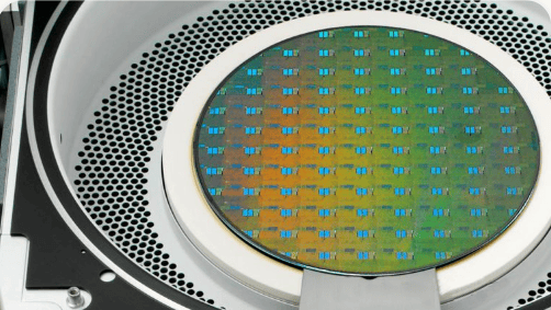
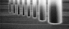
Loading effect refers to the phenomenon that when the etching area increases or the etching depth increases during dry etching, the etching rate decreases or the etching is uneven due to insufficient supply of reactive plasma. This effect is usually related to the characteristics of the etching system, such as plasma density and uniformity, vacuum degree, etc., and is widely present in various reactive ion etching.
• Improve plasma density and uniformity: By optimizing the design of the plasma source, such as using more efficient RF power or magnetron sputtering technology, a higher density and more uniformly distributed plasma can be generated.
• Adjust the composition of the reactive gas: Adding an appropriate amount of auxiliary gas to the reactive gas can improve the uniformity of the plasma and promote the effective discharge of etching byproducts.
• Optimize the vacuum system: Enhancing the pumping speed and efficiency of the vacuum pump can help reduce the residence time of etching byproducts in the chamber, thereby reducing the load effect.
• Design a reasonable photolithography layout: When designing the photolithography layout, the density of the pattern should be taken into account to avoid over-dense arrangement in local areas to reduce the impact of the load effect.
Ⅱ Micro-trenching effect
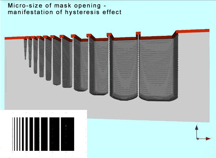
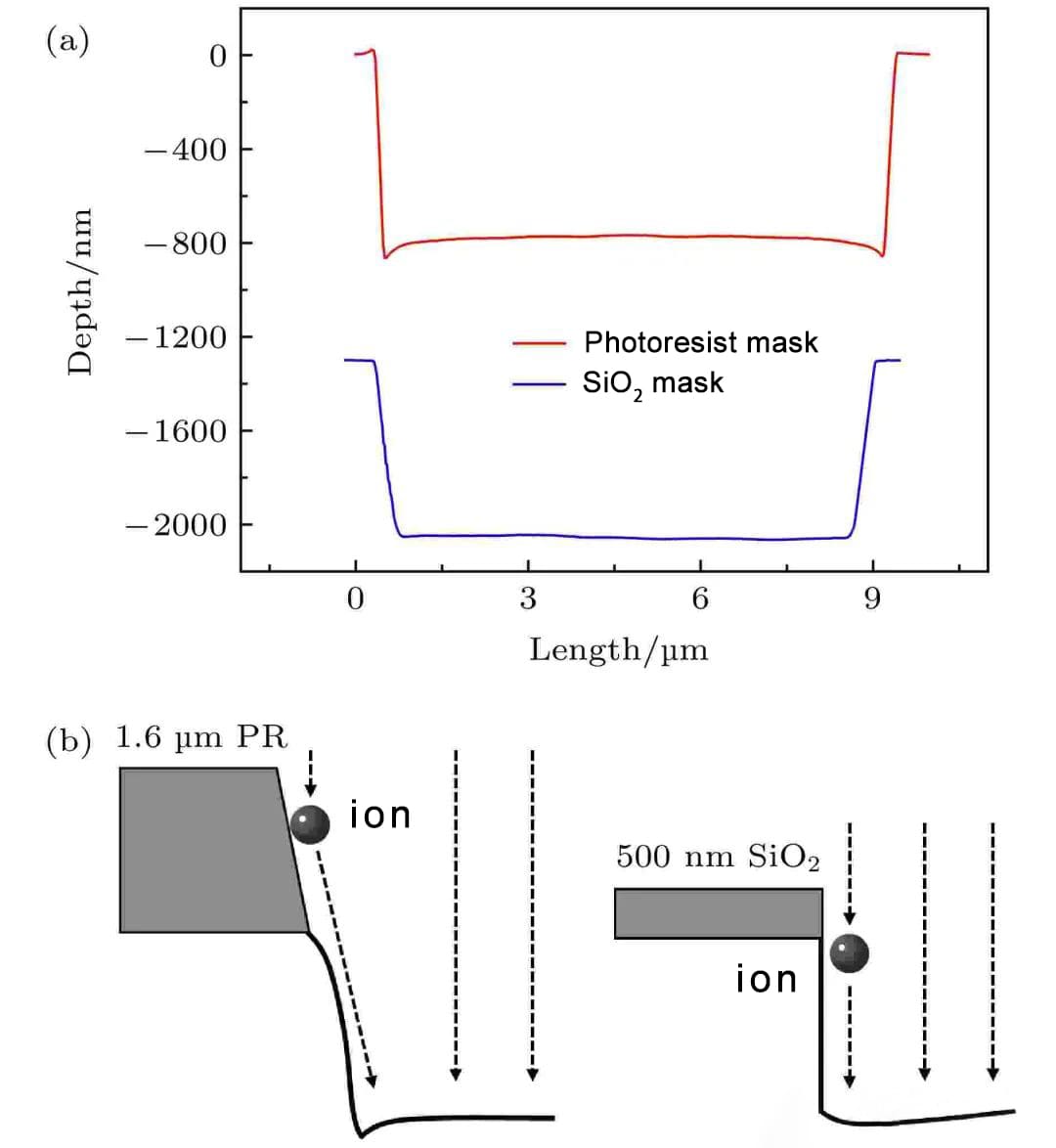
The micro-trenching effect refers to the phenomenon that during the etching process, due to the high-energy particles hitting the etching surface at an inclined angle, the etching rate near the side wall is higher than that in the central area, resulting in non-vertical chamfers on the side wall. This phenomenon is closely related to the angle of the incident particles and the slope of the side wall.
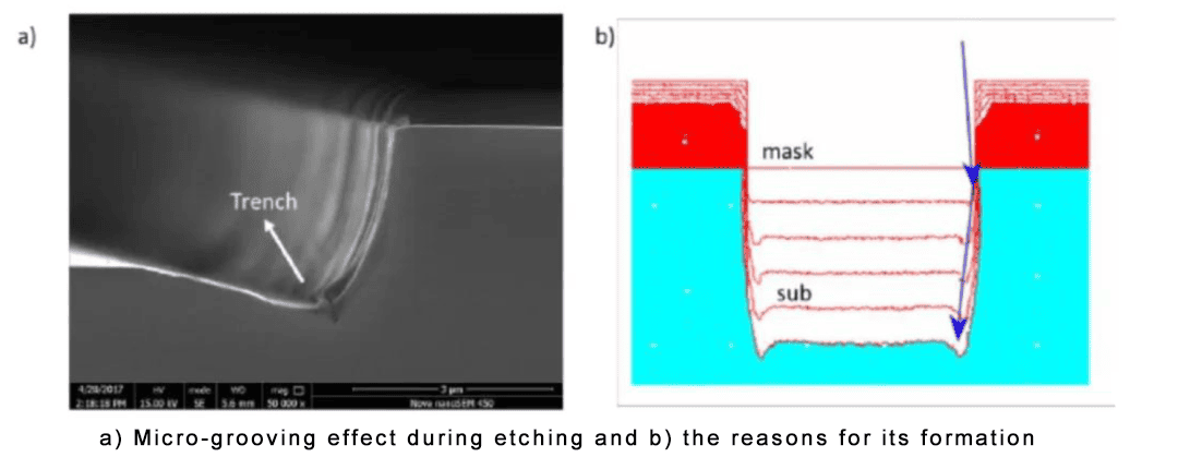
• Increase RF power: Properly increasing the RF power can increase the energy of the incident particles, allowing them to bombard the target surface more vertically, thereby reducing the etching rate difference of the side wall.
• Choose the right etching mask material: Some materials can better resist the charging effect and reduce the micro-trenching effect aggravated by the accumulation of negative charge on the mask.
• Optimize etching conditions: By finely adjusting parameters such as temperature and pressure during the etching process, the selectivity and uniformity of etching can be effectively controlled.
Ⅲ Charging Effect
The charging effect is caused by the insulating properties of the etching mask. When the electrons in the plasma cannot escape quickly, they will gather on the mask surface to form a local electric field, interfere with the path of the incident particles, and affect the anisotropy of etching, especially when etching fine structures.
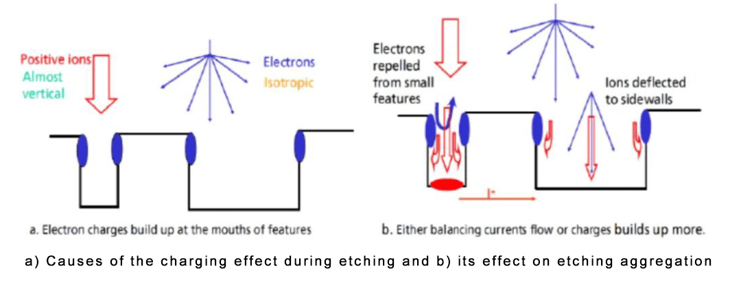
• Select suitable etching mask materials: Some specially treated materials or conductive mask layers can effectively reduce the aggregation of electrons.
• Implement intermittent etching: By periodically interrupting the etching process and giving electrons enough time to escape, the charging effect can be significantly reduced.
• Adjust the etching environment: Changing the gas composition, pressure and other conditions in the etching environment can help improve the stability of the plasma and reduce the occurrence of the charging effect.
