- English
- Español
- Português
- русский
- Français
- 日本語
- Deutsch
- tiếng Việt
- Italiano
- Nederlands
- ภาษาไทย
- Polski
- 한국어
- Svenska
- magyar
- Malay
- বাংলা ভাষার
- Dansk
- Suomi
- हिन्दी
- Pilipino
- Türkçe
- Gaeilge
- العربية
- Indonesia
- Norsk
- تمل
- český
- ελληνικά
- український
- Javanese
- فارسی
- தமிழ்
- తెలుగు
- नेपाली
- Burmese
- български
- ລາວ
- Latine
- Қазақша
- Euskal
- Azərbaycan
- Slovenský jazyk
- Македонски
- Lietuvos
- Eesti Keel
- Română
- Slovenski
- मराठी
- Srpski језик
What is the difference between silicon carbide (SiC) and gallium nitride (GaN) applications? - VeTek Semiconductor
2024-10-10
![]()
SiC and GaN are referred to as "wide bandgap semiconductors" (WBG). Due to the production process used, WBG devices show the following advantages:
1. Wide Bandgap Semiconductors
Gallium nitride (GaN) and silicon carbide (SiC) are relatively similar in terms of bandgap and breakdown field. The bandgap of gallium nitride is 3.2 eV, while the bandgap of silicon carbide is 3.4 eV. Although these values appear similar, they are significantly higher than the bandgap of silicon. The bandgap of silicon is only 1.1 eV, which is three times smaller than that of gallium nitride and silicon carbide. The higher bandgaps of these compounds allow gallium nitride and silicon carbide to comfortably support higher voltage circuits, but they cannot support low voltage circuits like silicon.
2. Breakdown Field Strength
The breakdown fields of gallium nitride and silicon carbide are relatively similar, with gallium nitride having a breakdown field of 3.3 MV/cm and silicon carbide having a breakdown field of 3.5 MV/cm. These breakdown fields allow the compounds to handle higher voltages significantly better than regular silicon. Silicon has a breakdown field of 0.3 MV/cm, which means that GaN and SiC are almost ten times more capable of sustaining higher voltages. They are also able to support lower voltages using significantly smaller devices.
3. High Electron Mobility Transistor (HEMT)
The most significant difference between GaN and SiC is their electron mobility, which indicates how fast electrons move through the semiconductor material. First, silicon has an electron mobility of 1500 cm^2/Vs. GaN has an electron mobility of 2000 cm^2/Vs, which means that electrons move more than 30% faster than silicon's electrons. However, SiC has an electron mobility of 650 cm^2/Vs, which means that SiC's electrons move slower than GaN and Si's electrons. With such a high electron mobility, GaN is almost three times more capable for high-frequency applications. Electrons can move through GaN semiconductors much faster than SiC.
4. Thermal Conductivity of GaN and SiC
The thermal conductivity of a material is its ability to transfer heat through itself. Thermal conductivity directly affects the temperature of a material, given the environment in which it is used. In high-power applications, the inefficiency of the material generates heat, which raises the material's temperature and subsequently changes its electrical properties. GaN has a thermal conductivity of 1.3 W/cmK, which is actually worse than that of silicon, which has a conductivity of 1.5 W/cmK. However, SiC has a thermal conductivity of 5 W/cmK, making it nearly three times better at transferring heat loads. This property makes SiC highly advantageous in high-power, high-temperature applications.
5. Semiconductor Wafer Manufacturing Process
Current manufacturing processes are a limiting factor for GaN and SiC because they are more expensive, less precise, or more energy-intensive than the widely adopted silicon manufacturing processes. For example, GaN contains a large number of crystal defects over a small area. Silicon, on the other hand, can only contain 100 defects per square centimeter. Obviously, this huge defect rate makes GaN inefficient. While manufacturers have made great strides in recent years, GaN is still struggling to meet the stringent semiconductor design requirements.
6. Power Semiconductor Market
Compared to silicon, current manufacturing technology limits the cost-effectiveness of gallium nitride and silicon carbide, making both high-power materials more expensive in the short term. However, both materials have strong advantages in specific semiconductor applications.
Silicon carbide may be a more effective product in the short term because it is easier to manufacture larger and more uniform SiC wafers than gallium nitride. Over time, gallium nitride will find its place in small, high-frequency products given its higher electron mobility. Silicon carbide will be more desirable in larger power products because its power capabilities are higher than gallium nitride's thermal conductivity.
![]()
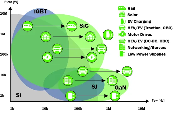
Gallium nitride and silicon carbide devices compete with silicon semiconductor (LDMOS) MOSFETs and superjunction MOSFETs. GaN and SiC devices are similar in some ways, but there are also significant differences.

Figure 1. The relationship between high voltage, high current, switching frequency, and major application areas.
Wide Bandgap Semiconductors
WBG compound semiconductors have higher electron mobility and higher bandgap energy, which translates into superior properties over silicon. Transistors made from WBG compound semiconductors have higher breakdown voltages and tolerance to high temperatures. These devices offer advantages over silicon in high-voltage and high-power applications.
![]()
Figure 2. A dual-die dual-FET cascade circuit converts a GaN transistor into a normally-off device, enabling standard enhancement-mode operation in high-power switching circuits
WBG transistors also switch faster than silicon and can operate at higher frequencies. Lower “on” resistance means they dissipate less power, improving energy efficiency. This unique combination of characteristics makes these devices attractive for some of the most demanding circuits in automotive applications, particularly hybrid and electric vehicles.
GaN and SiC transistors to meet challenges in automotive electrical equipment
Key benefits of GaN and SiC devices: High voltage capability, with 650 V, 900 V and 1200 V devices,
Silicon carbide:
Higher 1700V.3300V and 6500V.
Faster switching speeds,
Higher operating temperatures.
Lower on resistance, minimal power dissipation, and higher energy efficiency.
GaN Devices
In switching applications, enhancement-mode (or E-mode) devices, which are usually “off”, are preferred, which led to the development of E-mode GaN devices. First came the cascade of two FET devices (Figure 2). Now, standard e-mode GaN devices are available. They can switch at frequencies up to 10 MHz and power levels up to tens of kilowatts.
GaN devices are widely used in wireless equipment as power amplifiers at frequencies up to 100 GHz. Some of the main use cases are cellular base station power amplifiers, military radars, satellite transmitters, and general RF amplification. However, due to high voltage (up to 1,000 V), high temperature, and fast switching, they are also incorporated into various switching power applications such as DC-DC converters, inverters, and battery chargers.
SiC Devices
SiC transistors are natural E-mode MOSFETs. These devices can switch at frequencies up to 1 MHz and at voltage and current levels much higher than silicon MOSFETs. Maximum drain-source voltage is up to about 1,800 V, and current capability is 100 amps. Additionally, SiC devices have a much lower on-resistance than silicon MOSFETs, resulting in higher efficiency in all switching power supply applications (SMPS designs).
SiC devices require a gate voltage drive of 18 to 20 volts to turn on the device with low on-resistance. Standard Si MOSFETs require less than 10 volts at the gate to fully turn on. Additionally, SiC devices require a -3 to -5 V gate drive to switch to the off state. The high voltage, high current capabilities of SiC MOSFETs make them ideal for automotive power circuits.
In many applications, IGBTs are being replaced by SiC devices. SiC devices can switch at higher frequencies, reducing the size and cost of inductors or transformers while improving efficiency. Additionally, SiC can handle higher currents than GaN.
There is competition between GaN and SiC devices, especially silicon LDMOS MOSFETs, superjunction MOSFETs, and IGBTs. In many applications, they are being replaced by GaN and SiC transistors.
To summarize the GaN vs. SiC comparison, here are the highlights:
GaN switches faster than Si.
SiC operates at higher voltages than GaN.
SiC requires high gate drive voltages.
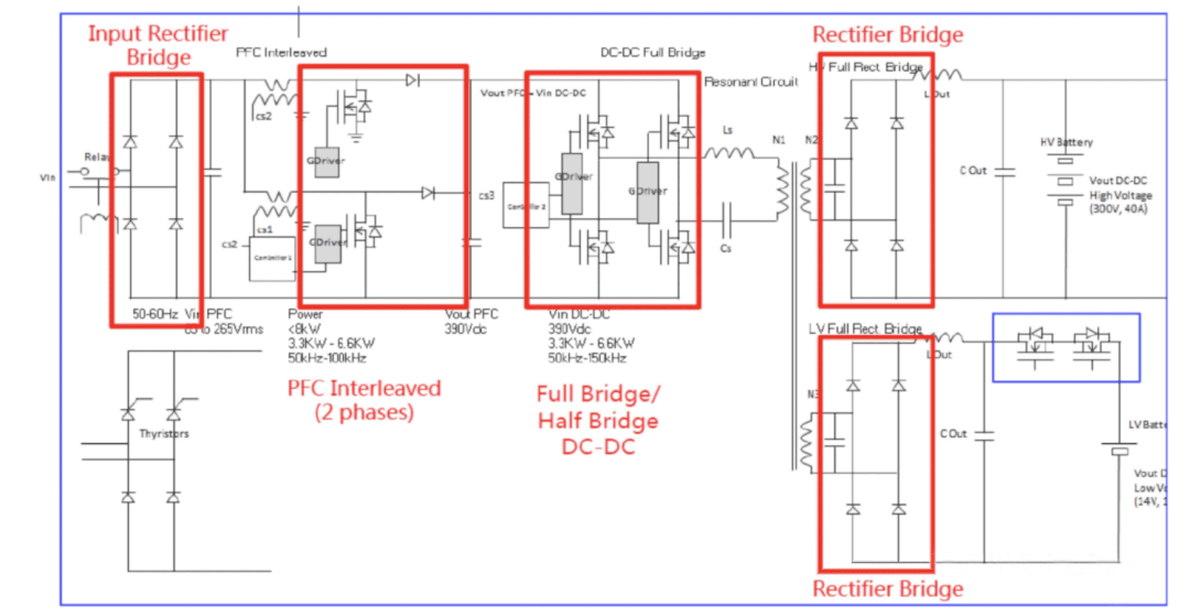
Many power circuits and devices can be improved by designing with GaN and SiC. One of the biggest beneficiaries is the automotive electrical system. Modern hybrid and electric vehicles contain devices that can use these devices. Some of the popular applications are OBCs, DC-DC converters, motor drives, and LiDAR. Figure 3 points out the main subsystems in electric vehicles that require high power switching transistors.

Figure 3. WBG on-board charger (OBC) for hybrid and electric vehicles. The AC input is rectified, power factor corrected (PFC), and then DC-DC converted
DC-DC converter. This is a power circuit that converts the high battery voltage to a lower voltage to run other electrical devices. Today's battery voltage ranges up to 600V or 900V. The DC-DC converter steps it down to 48V or 12V, or both, for the operation of other electronic components (Figure 3). In hybrid electric and electric vehicles (HEVEVs), DC-DC can also be used for the high-voltage bus between the battery pack and the inverter.
On-board chargers (OBCs). Plug-in HEVEVs and EVs contain an internal battery charger that can be connected to an AC mains supply. This allows charging at home without the need for an external AC−DC charger (Figure 4).
Main drive motor driver. The main drive motor is a high-output AC motor that drives the vehicle's wheels. The driver is an inverter that converts the battery voltage to three-phase AC to turn the motor.

Figure 4. A typical DC-DC converter is used to convert high battery voltages to 12 V and/or 48 V. IGBTs used in high-voltage bridges are being replaced by SiC MOSFETs.
GaN and SiC transistors offer automotive electrical designers flexibility and simpler designs as well as superior performance due to their high voltage, high current, and fast switching characteristics.
VeTek Semiconductor is a professional Chinese manufacturer of Tantalum Carbide Coating, Silicon Carbide Coating, GaN products, Special Graphite, Silicon Carbide Ceramics and Other Semiconductor Ceramics. VeTek Semiconductor is committed to providing advanced solutions for various Coating products for the semiconductor industry.
If you have any inquiries or need additional details, please don't hesitate to get in touch with us.
Mob/WhatsAPP: +86-180 6922 0752
Email: anny@veteksemi.com


