
- English
- Español
- Português
- русский
- Français
- 日本語
- Deutsch
- tiếng Việt
- Italiano
- Nederlands
- ภาษาไทย
- Polski
- 한국어
- Svenska
- magyar
- Malay
- বাংলা ভাষার
- Dansk
- Suomi
- हिन्दी
- Pilipino
- Türkçe
- Gaeilge
- العربية
- Indonesia
- Norsk
- تمل
- český
- ελληνικά
- український
- Javanese
- فارسی
- தமிழ்
- తెలుగు
- नेपाली
- Burmese
- български
- ລາວ
- Latine
- Қазақша
- Euskal
- Azərbaycan
- Slovenský jazyk
- Македонски
- Lietuvos
- Eesti Keel
- Română
- Slovenski
- मराठी
- Srpski језик
A complete explanation of the chip manufacturing process (2/2): from wafer to packaging and testing
2024-09-18
The manufacturing of each semiconductor product requires hundreds of processes, and the entire manufacturing process is divided into eight steps: wafer processing - oxidation - photolithography - etching - thin film deposition - interconnection - testing - packaging.
Step 5: Thin film deposition
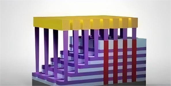
In order to create the micro devices inside the chip, we need to continuously deposit layers of thin films and remove the excess parts by etching, and also add some materials to separate different devices. Each transistor or memory cell is built step by step through the above process. The "thin film" we are talking about here refers to a "film" with a thickness of less than 1 micron (μm, one millionth of a meter) that cannot be manufactured by ordinary mechanical processing methods. The process of placing a film containing the required molecular or atomic units on a wafer is "deposition".
To form a multi-layer semiconductor structure, we need to first make a device stack, that is, alternately stack multiple layers of thin metal (conductive) films and dielectric (insulating) films on the surface of the wafer, and then remove the excess parts through repeated etching processes to form a three-dimensional structure. Techniques that can be used for deposition processes include chemical vapor deposition (CVD), atomic layer deposition (ALD), and physical vapor deposition (PVD), and methods using these techniques can be divided into dry and wet deposition.
Chemical vapor deposition(CVD)
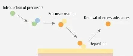
In chemical vapor deposition, precursor gases react in a reaction chamber to form a thin film attached to the surface of the wafer and byproducts that are pumped out of the chamber. Plasma-enhanced chemical vapor deposition uses plasma to generate the reactant gases. This method reduces the reaction temperature, making it ideal for temperature-sensitive structures. Using plasma can also reduce the number of depositions, often resulting in higher-quality films.
Atomic layer deposition(ALD)
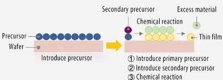
Atomic layer deposition forms thin films by depositing only a few atomic layers at a time. The key to this method is to cycle independent steps that are performed in a certain order and maintain good control. Coating the wafer surface with a precursor is the first step, and then different gases are introduced to react with the precursor to form the desired substance on the wafer surface.
Physical vapor deposition(PVD)
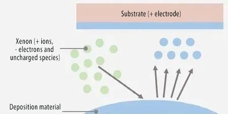
As the name implies, physical vapor deposition refers to the formation of thin films by physical means. Sputtering is a physical vapor deposition method that uses argon plasma to sputter atoms from a target and deposit them on the surface of a wafer to form a thin film. In some cases, the deposited film can be treated and improved through techniques such as ultraviolet thermal treatment (UVTP).
Step 6: Interconnection
The conductivity of semiconductors is between conductors and non-conductors (i.e. insulators), which allows us to fully control the flow of electricity. Wafer-based lithography, etching and deposition processes can build components such as transistors, but they need to be connected to enable the transmission and reception of power and signals.
Metals are used for circuit interconnection because of their conductivity. Metals used for semiconductors need to meet the following conditions:
· Low resistivity: Since metal circuits need to pass current, the metals in them should have low resistance.
· Thermochemical stability: The properties of metal materials must remain unchanged during the metal interconnection process.
· High reliability: As integrated circuit technology develops, even small amounts of metal interconnect materials must have sufficient durability.
· Manufacturing cost: Even if the first three conditions are met, the material cost is too high to meet the needs of mass production.
The interconnection process mainly uses two materials, aluminum and copper.
Aluminum Interconnection Process
The aluminum interconnection process begins with aluminum deposition, photoresist application, exposure and development, followed by etching to selectively remove any excess aluminum and photoresist before entering the oxidation process. After the above steps are completed, the photolithography, etching and deposition processes are repeated until the interconnection is completed.
In addition to its excellent conductivity, aluminum is also easy to photolithograph, etch and deposit. In addition, it has a low cost and good adhesion to the oxide film. Its disadvantages are that it is easy to corrode and has a low melting point. In addition, to prevent aluminum from reacting with silicon and causing connection problems, metal deposits need to be added to separate aluminum from the wafer. This deposit is called "barrier metal".
Aluminum circuits are formed by deposition. After the wafer enters the vacuum chamber, a thin film formed by aluminum particles will adhere to the wafer. This process is called "vapor deposition (VD)", which includes chemical vapor deposition and physical vapor deposition.

Copper Interconnection Process
As semiconductor processes become more sophisticated and device sizes shrink, the connection speed and electrical properties of aluminum circuits are no longer adequate, and new conductors that meet both size and cost requirements are needed. The first reason copper can replace aluminum is that it has lower resistance, which allows for faster device connection speeds. Copper is also more reliable because it is more resistant to electromigration, the movement of metal ions when current flows through a metal, than aluminum.
However, copper does not easily form compounds, making it difficult to vaporize and remove from the surface of a wafer. To address this problem, instead of etching copper, we deposit and etch dielectric materials, which form metal line patterns consisting of trenches and vias where needed, and then fill the aforementioned "patterns" with copper to achieve interconnection, a process called "damascene".
As copper atoms continue to diffuse into the dielectric, the latter's insulation decreases and creates a barrier layer that blocks the copper atoms from further diffusion. A thin copper seed layer is then formed on the barrier layer. This step allows electroplating, which is the filling of high aspect ratio patterns with copper. After filling, the excess copper can be removed by metal chemical mechanical polishing (CMP). After completion, an oxide film can be deposited, and the excess film can be removed by photolithography and etching processes. The above process needs to be repeated until the copper interconnection is completed.
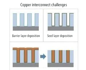
From the above comparison, it can be seen that the difference between copper interconnection and aluminum interconnection is that the excess copper is removed by metal CMP rather than etching.
Step 7: Testing
The main goal of the test is to verify whether the quality of the semiconductor chip meets a certain standard, so as to eliminate defective products and improve the reliability of the chip. In addition, defective products tested will not enter the packaging step, which helps to save cost and time. Electronic die sorting (EDS) is a test method for wafers.
EDS is a process that verifies the electrical characteristics of each chip in the wafer state and thereby improves the semiconductor yield. EDS can be divided into five steps, as follows:
01 Electrical parameter monitoring (EPM)
EPM is the first step in semiconductor chip testing. This step will test each device (including transistors, capacitors, and diodes) required for semiconductor integrated circuits to ensure that their electrical parameters meet the standards. The main function of EPM is to provide measured electrical characteristic data, which will be used to improve the efficiency of semiconductor manufacturing processes and product performance (not to detect defective products).
02 Wafer Aging Test
The semiconductor defect rate comes from two aspects, namely the rate of manufacturing defects (higher in the early stage) and the rate of defects in the entire life cycle. Wafer aging test refers to testing the wafer under a certain temperature and AC/DC voltage to find out the products that may have defects in the early stage, that is, to improve the reliability of the final product by discovering potential defects.
03 Detection
After the aging test is completed, the semiconductor chip needs to be connected to the test device with a probe card, and then the temperature, speed and motion tests can be performed on the wafer to verify the relevant semiconductor functions. Please see the table for a description of the specific test steps.
04 Repair
Repair is the most important test step because some defective chips can be repaired by replacing the problematic components.
05 Dotting
The chips that failed the electrical test have been sorted out in the previous steps, but they still need to be marked to distinguish them. In the past, we needed to mark defective chips with special ink to ensure that they could be identified with the naked eye, but now the system automatically sorts them according to the test data value.
Step 8: Packaging
After the previous several processes, the wafer will form square chips of equal size (also known as "single chips"). The next thing to do is to obtain individual chips by cutting. The newly cut chips are very fragile and cannot exchange electrical signals, so they need to be processed separately. This process is packaging, which includes forming a protective shell outside the semiconductor chip and allowing them to exchange electrical signals with the outside. The entire packaging process is divided into five steps, namely wafer sawing, single chip attachment, interconnection, molding and packaging testing.
01 Wafer sawing
In order to cut countless densely arranged chips from the wafer, we must first carefully "grind" the back of the wafer until its thickness meets the needs of the packaging process. After grinding, we can cut along the scribe line on the wafer until the semiconductor chip is separated.
There are three types of wafer sawing technology: blade cutting, laser cutting and plasma cutting. Blade dicing is the use of a diamond blade to cut the wafer, which is prone to frictional heat and debris and thus damage the wafer. Laser dicing has higher precision and can easily handle wafers with thin thickness or small scribe line spacing. Plasma dicing uses the principle of plasma etching, so this technology is also applicable even if the scribe line spacing is very small.
02 Single Wafer Attachment
After all chips are separated from the wafer, we need to attach the individual chips (single wafers) to the substrate (lead frame). The function of the substrate is to protect the semiconductor chips and enable them to exchange electrical signals with external circuits. Liquid or solid tape adhesives can be used to attach the chips.
03 Interconnection
After attaching the chip to the substrate, we also need to connect the contact points of the two to achieve electrical signal exchange. There are two connection methods that can be used in this step: wire bonding using thin metal wires and flip chip bonding using spherical gold blocks or tin blocks. Wire bonding is a traditional method, and flip chip bonding technology can speed up semiconductor manufacturing.
04 Molding
After completing the connection of the semiconductor chip, a molding process is needed to add a package to the outside of the chip to protect the semiconductor integrated circuit from external conditions such as temperature and humidity. After the package mold is made as needed, we need to put the semiconductor chip and epoxy molding compound (EMC) into the mold and seal it. The sealed chip is the final form.
05 Packaging Test
The chips that have already had their final form must also pass the final defect test. All the finished semiconductor chips that enter the final test are finished semiconductor chips. They will be placed in the test equipment and set different conditions such as voltage, temperature and humidity for electrical, functional and speed tests. The results of these tests can be used to find defects and improve product quality and production efficiency.
Evolution of packaging technology
As chip size decreases and performance requirements increase, packaging has undergone many technological innovations in the past few years. Some future-oriented packaging technologies and solutions include the use of deposition for traditional back-end processes such as wafer-level packaging (WLP), bumping processes and redistribution layer (RDL) technology, as well as etching and cleaning technologies for front-end wafer manufacturing.

What is advanced packaging?
Traditional packaging requires each chip to be cut out of the wafer and placed in a mold. Wafer-level packaging (WLP) is a type of advanced packaging technology, which refers to directly packaging the chip still on the wafer. The process of WLP is to package and test first, and then separate all the formed chips from the wafer at one time. Compared with traditional packaging, the advantage of WLP is lower production cost.
Advanced packaging can be divided into 2D packaging, 2.5D packaging and 3D packaging.
Smaller 2D packaging
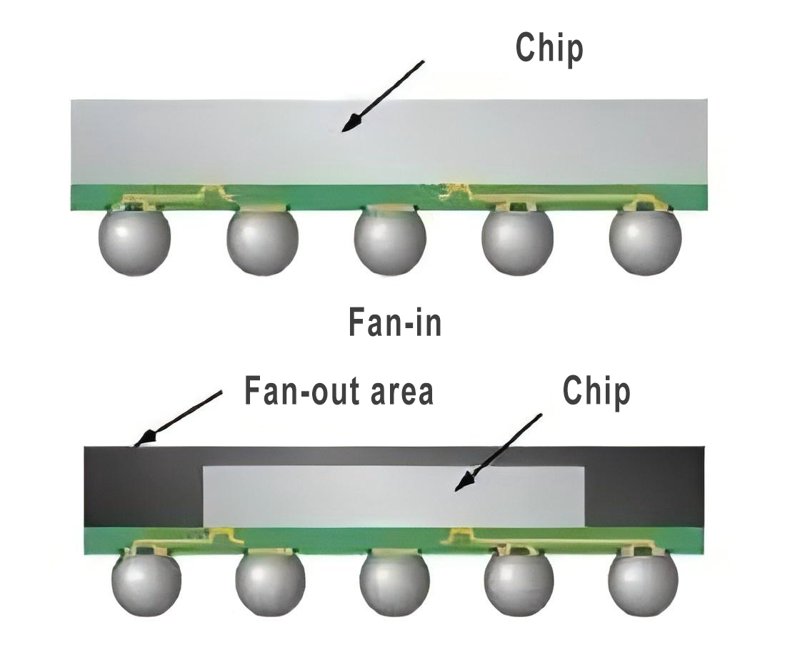
As mentioned earlier, the main purpose of the packaging process includes sending the signal of the semiconductor chip to the outside, and the bumps formed on the wafer are the contact points for sending input/output signals. These bumps are divided into fan-in and fan-out. The former fan-shaped is inside the chip, and the latter fan-shaped is beyond the chip range. We call the input/output signal I/O (input/output), and the number of input/output is called I/O count. I/O count is an important basis for determining the packaging method. If the I/O count is low, fan-in packaging is used. Since the chip size does not change much after packaging, this process is also called chip-scale packaging (CSP) or wafer-level chip-scale packaging (WLCSP). If the I/O count is high, fan-out packaging is usually used, and redistribution layers (RDLs) are required in addition to bumps to enable signal routing. This is "fan-out wafer-level packaging (FOWLP)."
2.5D packaging
2.5D packaging technology can put two or more types of chips into a single package while allowing signals to be routed laterally, which can increase the size and performance of the package. The most widely used 2.5D packaging method is to put memory and logic chips into a single package through a silicon interposer. 2.5D packaging requires core technologies such as through-silicon vias (TSVs), micro bumps, and fine-pitch RDLs.

3D packaging
3D packaging technology can put two or more types of chips into a single package while allowing signals to be routed vertically. This technology is suitable for smaller and higher I/O count semiconductor chips. TSV can be used for chips with high I/O counts, and wire bonding can be used for chips with low I/O counts, and ultimately form a signal system in which the chips are arranged vertically. The core technologies required for 3D packaging include TSV and micro-bump technology.
So far, the eight steps of semiconductor product manufacturing "wafer processing - oxidation - photolithography - etching - thin film deposition - interconnection - testing - packaging" have been fully introduced. From "sand" to "chips", semiconductor technology is performing a real version of "turning stones into gold".
VeTek Semiconductor is a professional Chinese manufacturer of Tantalum Carbide Coating, Silicon Carbide Coating, Special Graphite, Silicon Carbide Ceramics and Other Semiconductor Ceramics. VeTek Semiconductor is committed to providing advanced solutions for various SiC Wafer products for the semiconductor industry.
If you are interested in the above products , please feel free to contact us directly.
Mob: +86-180 6922 0752
WhatsAPP: +86 180 6922 0752
Email: anny@veteksemi.com


