- English
- Español
- Português
- русский
- Français
- 日本語
- Deutsch
- tiếng Việt
- Italiano
- Nederlands
- ภาษาไทย
- Polski
- 한국어
- Svenska
- magyar
- Malay
- বাংলা ভাষার
- Dansk
- Suomi
- हिन्दी
- Pilipino
- Türkçe
- Gaeilge
- العربية
- Indonesia
- Norsk
- تمل
- český
- ελληνικά
- український
- Javanese
- فارسی
- தமிழ்
- తెలుగు
- नेपाली
- Burmese
- български
- ລາວ
- Latine
- Қазақша
- Euskal
- Azərbaycan
- Slovenský jazyk
- Македонски
- Lietuvos
- Eesti Keel
- Română
- Slovenski
- मराठी
- Srpski језик
A complete explanation of the chip manufacturing process (1/2): from wafer to packaging and testing
2024-09-18
The manufacturing of each semiconductor product requires hundreds of processes, and the entire manufacturing process is divided into eight steps: wafer processing - oxidation - photolithography - etching - thin film deposition - interconnection - testing - packaging.
![]()
Step 1: Wafer processing
All semiconductor processes start with a grain of sand! Because the silicon contained in the sand is the raw material needed to produce wafers. Wafers are round slices cut from single crystal cylinders made of silicon (Si) or gallium arsenide (GaAs). To extract high-purity silicon materials, silica sand, a special material with a silicon dioxide content of up to 95%, is needed, which is also the main raw material for making wafers. Wafer processing is the process of making the above wafers.
Ingot casting
First, the sand needs to be heated to separate the carbon monoxide and silicon in it, and the process is repeated until ultra-high purity electronic grade silicon (EG-Si) is obtained. High-purity silicon melts into liquid and then solidifies into a single crystal solid form, called an "ingot", which is the first step in semiconductor manufacturing.
The manufacturing precision of silicon ingots (silicon pillars) is very high, reaching the nanometer level, and the widely used manufacturing method is the Czochralski method.
Ingot cutting
After the previous step is completed, it is necessary to cut off the two ends of the ingot with a diamond saw and then cut it into thin slices of a certain thickness. The diameter of the ingot slice determines the size of the wafer. Larger and thinner wafers can be divided into more usable units, which helps to reduce production costs. After cutting the silicon ingot, it is necessary to add "flat area" or "dent" marks on the slices to facilitate setting the processing direction as a standard in subsequent steps.
Wafer surface polishing
The slices obtained through the above cutting process are called "bare wafers", that is, unprocessed "raw wafers". The surface of the bare wafer is uneven and the circuit pattern cannot be printed directly on it. Therefore, it is necessary to first remove surface defects through grinding and chemical etching processes, then polish to form a smooth surface, and then remove residual contaminants through cleaning to obtain a finished wafer with a clean surface.
Step 2: Oxidation
The role of the oxidation process is to form a protective film on the surface of the wafer. It protects the wafer from chemical impurities, prevents leakage current from entering the circuit, prevents diffusion during ion implantation, and prevents the wafer from slipping during etching.
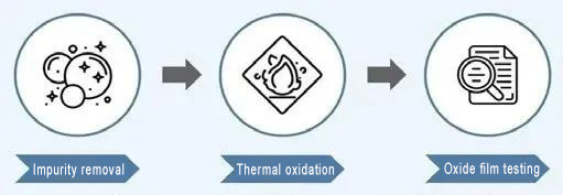
The first step of the oxidation process is to remove impurities and contaminants. It requires four steps to remove organic matter, metal impurities and evaporate residual water. After cleaning, the wafer can be placed in a high temperature environment of 800 to 1200 degrees Celsius, and a silicon dioxide (i.e. "oxide") layer is formed by the flow of oxygen or steam on the surface of the wafer. Oxygen diffuses through the oxide layer and reacts with silicon to form an oxide layer of varying thickness, and its thickness can be measured after oxidation is completed.
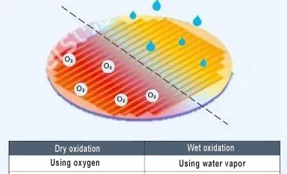
Dry oxidation and wet oxidation Depending on the different oxidants in the oxidation reaction, the thermal oxidation process can be divided into dry oxidation and wet oxidation. The former uses pure oxygen to produce a silicon dioxide layer, which is slow but the oxide layer is thin and dense. The latter requires both oxygen and highly soluble water vapor, which is characterized by a fast growth rate but a relatively thick protective layer with a low density.
In addition to the oxidant, there are other variables that affect the thickness of the silicon dioxide layer. First, the wafer structure, its surface defects and internal doping concentration will affect the rate of oxide layer generation. In addition, the higher the pressure and temperature generated by the oxidation equipment, the faster the oxide layer will be generated. During the oxidation process, it is also necessary to use a dummy sheet according to the position of the wafer in the unit to protect the wafer and reduce the difference in oxidation degree.
Step 3: Photolithography
Photolithography is to "print" the circuit pattern onto the wafer through light. We can understand it as drawing the plane map required for semiconductor manufacturing on the surface of the wafer. The higher the fineness of the circuit pattern, the higher the integration of the finished chip, which must be achieved through advanced photolithography technology. Specifically, photolithography can be divided into three steps: coating photoresist, exposure and development.
Coating
The first step of drawing a circuit on a wafer is to coat the photoresist on the oxide layer. Photoresist makes the wafer a "photo paper" by changing its chemical properties. The thinner the photoresist layer on the surface of the wafer, the more uniform the coating, and the finer the pattern that can be printed. This step can be done by the "spin coating" method. According to the difference in light (ultraviolet) reactivity, photoresists can be divided into two types: positive and negative. The former will decompose and disappear after exposure to light, leaving the pattern of the unexposed area, while the latter will polymerize after exposure to light and make the pattern of the exposed part appear.
Exposure
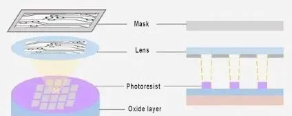
After the photoresist film is covered on the wafer, the circuit printing can be completed by controlling the light exposure. This process is called "exposure". We can selectively pass light through the exposure equipment. When the light passes through the mask containing the circuit pattern, the circuit can be printed on the wafer coated with the photoresist film below.
During the exposure process, the finer the printed pattern, the more components the final chip can accommodate, which helps to improve production efficiency and reduce the cost of each component. In this field, the new technology that is currently attracting much attention is EUV lithography. Lam Research Group has jointly developed a new dry film photoresist technology with strategic partners ASML and imec. This technology can greatly improve the productivity and yield of EUV lithography exposure process by improving resolution (a key factor in fine-tuning circuit width).
Development
The step after exposure is to spray the developer on the wafer, the purpose is to remove the photoresist in the uncovered area of the pattern, so that the printed circuit pattern can be revealed. After the development is completed, it needs to be checked by various measuring equipment and optical microscopes to ensure the quality of the circuit diagram.
Step 4: Etching
After the photolithography of the circuit diagram is completed on the wafer, an etching process is used to remove any excess oxide film and leave only the semiconductor circuit diagram. To do this, liquid, gas or plasma is used to remove the selected excess parts. There are two main methods of etching, depending on the substances used: wet etching using a specific chemical solution to chemically react to remove the oxide film, and dry etching using gas or plasma.
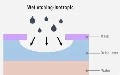
Wet etching
Wet etching using chemical solutions to remove oxide films has the advantages of low cost, fast etching speed and high productivity. However, wet etching is isotropic, that is, its speed is the same in any direction. This causes the mask (or sensitive film) to not be completely aligned with the etched oxide film, so it is difficult to process very fine circuit diagrams.
Dry Etching
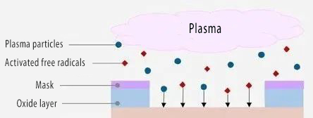
Dry etching can be divided into three different types. The first is chemical etching, which uses etching gases (mainly hydrogen fluoride). Like wet etching, this method is isotropic, which means it is not suitable for fine etching.
The second method is physical sputtering, which uses ions in the plasma to impact and remove the excess oxide layer. As an anisotropic etching method, sputtering etching has different etching rates in the horizontal and vertical directions, so its fineness is also better than chemical etching. However, the disadvantage of this method is that the etching speed is slow because it relies entirely on the physical reaction caused by ion collision.
The last third method is reactive ion etching (RIE). RIE combines the first two methods, that is, while using plasma for ionization physical etching, chemical etching is carried out with the help of free radicals generated after plasma activation. In addition to the etching speed exceeding the first two methods, RIE can use the anisotropic characteristics of ions to achieve high-precision pattern etching.
Today, dry etching has been widely used to improve the yield of fine semiconductor circuits. Maintaining full-wafer etching uniformity and increasing etching speed are critical, and today's most advanced dry etching equipment is supporting the production of the most advanced logic and memory chips with higher performance.

VeTek Semiconductor is a professional Chinese manufacturer of Tantalum Carbide Coating, Silicon Carbide Coating, Special Graphite, Silicon Carbide Ceramics and Other Semiconductor Ceramics. VeTek Semiconductor is committed to providing advanced solutions for various SiC Wafer products for the semiconductor industry.
If you are interested in the above products , please feel free to contact us directly.
Mob: +86-180 6922 0752
WhatsAPP: +86 180 6922 0752
Email: anny@veteksemi.com

