
- English
- Español
- Português
- русский
- Français
- 日本語
- Deutsch
- tiếng Việt
- Italiano
- Nederlands
- ภาษาไทย
- Polski
- 한국어
- Svenska
- magyar
- Malay
- বাংলা ভাষার
- Dansk
- Suomi
- हिन्दी
- Pilipino
- Türkçe
- Gaeilge
- العربية
- Indonesia
- Norsk
- تمل
- český
- ελληνικά
- український
- Javanese
- فارسی
- தமிழ்
- తెలుగు
- नेपाली
- Burmese
- български
- ລາວ
- Latine
- Қазақша
- Euskal
- Azərbaycan
- Slovenský jazyk
- Македонски
- Lietuvos
- Eesti Keel
- Română
- Slovenski
- मराठी
- Srpski језик

Different technical routes of SiC epitaxial growth furnace
2024-07-05
Silicon carbide substrates have many defects and cannot be processed directly. A specific single crystal thin film needs to be grown on them through an epitaxial process to make chip wafers. This thin film is the epitaxial layer. Almost all silicon carbide devices are realized on epitaxial materials. High-quality silicon carbide homogeneous epitaxial materials are the basis for the development of silicon carbide devices. The performance of epitaxial materials directly determines the realization of the performance of silicon carbide devices.
High-current and high-reliability silicon carbide devices have put forward more stringent requirements on the surface morphology, defect density, doping and thickness uniformity of epitaxial materials. Large-size, low-defect density and high-uniformity silicon carbide epitaxy has become the key to the development of the silicon carbide industry.
The preparation of high-quality silicon carbide epitaxy requires advanced processes and equipment. The most widely used silicon carbide epitaxial growth method is chemical vapor deposition (CVD), which has the advantages of precise control of epitaxial film thickness and doping concentration, fewer defects, moderate growth rate, and automatic process control. It is a reliable technology that has been successfully commercialized.
Silicon carbide CVD epitaxy generally uses hot wall or warm wall CVD equipment, which ensures the continuation of the epitaxial layer 4H crystal SiC under higher growth temperature conditions (1500-1700℃). After years of development, hot wall or warm wall CVD can be divided into horizontal horizontal structure reactors and vertical vertical structure reactors according to the relationship between the direction of the inlet gas flow and the substrate surface.
The quality of silicon carbide epitaxial furnace mainly has three indicators. The first is the epitaxial growth performance, including thickness uniformity, doping uniformity, defect rate and growth rate; the second is the temperature performance of the equipment itself, including heating/cooling rate, maximum temperature, temperature uniformity; and finally the cost performance of the equipment itself, including unit price and production capacity.
Differences between three types of silicon carbide epitaxial growth furnaces
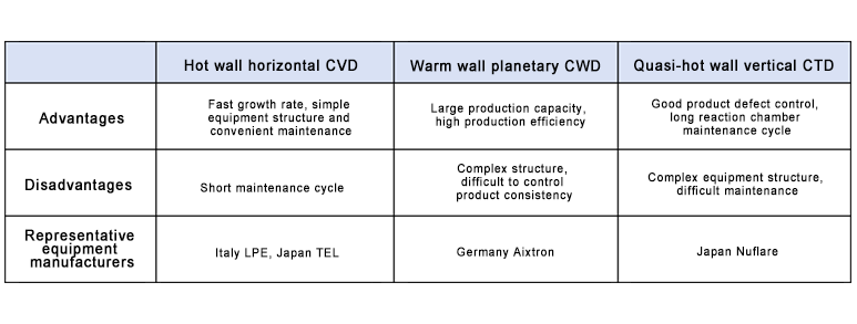
Hot wall horizontal CVD, warm wall planetary CVD and quasi-hot wall vertical CVD are the mainstream epitaxial equipment technology solutions that have been commercially applied at this stage. The three technical equipment also have their own characteristics and can be selected according to needs. The structure diagram is shown in the figure below:
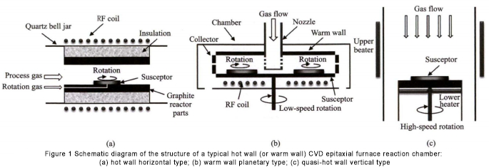
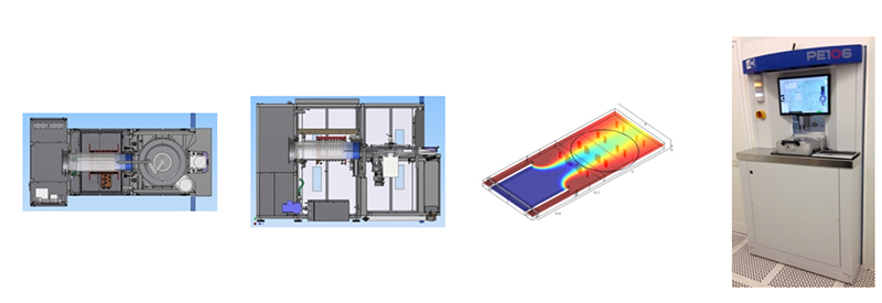
The hot wall horizontal CVD system is generally a single-wafer large-size growth system driven by air flotation and rotation. It is easy to achieve good in-wafer indicators. The representative model is Pe1O6 of LPE Company in Italy. This machine can realize automatic loading and unloading of wafers at 900℃. The main features are high growth rate, short epitaxial cycle, good consistency within the wafer and between furnaces, etc. It has the highest market share in China
According to LPE official reports, combined with the usage of major users, the 100-150mm (4-6 inches) 4H-SiC epitaxial wafer products with a thickness of less than 30μm produced by the Pe1O6 epitaxial furnace can stably achieve the following indicators: intra-wafer epitaxial thickness non-uniformity ≤2%, intra-wafer doping concentration non-uniformity ≤5%, surface defect density ≤1cm-2, surface defect-free area (2mm×2mm unit cell) ≥90%.
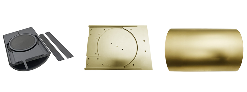
Domestic companies such as JSG, CETC 48, NAURA, and NASO have developed monolithic silicon carbide epitaxial equipment with similar functions and have achieved large-scale shipments. For example, in February 2023, JSG released a 6-inch double-wafer SiC epitaxial equipment. The equipment uses the upper and lower layers of the upper and lower layers of the graphite parts of the reaction chamber to grow two epitaxial wafers in a single furnace, and the upper and lower process gases can be separately regulated, with a temperature difference of ≤5°C, which effectively makes up for the disadvantage of insufficient production capacity of monolithic horizontal epitaxial furnaces.The key spare part is SiC Coating Halfmoon Parts.We are supplying 6 inch and 8 inch halfmoon parts to the users.
The warm-wall planetary CVD system, with a planetary arrangement of the base, is characterized by the growth of multiple wafers in a single furnace and high output efficiency. Representative models are the AIXG5WWC (8X150mm) and G10-SiC (9×150mm or 6×200mm) series epitaxial equipment of Aixtron of Germany.
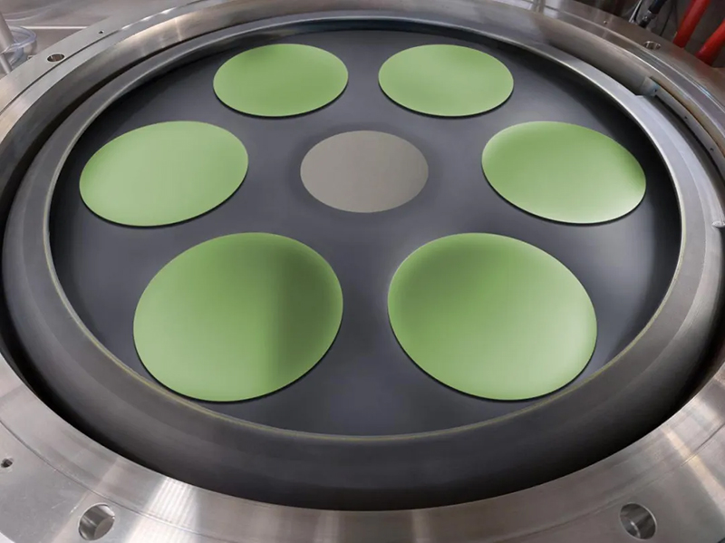
According to Aixtron's official report, the 6-inch 4H-SiC epitaxial wafer products with a thickness of 10μm produced by the G10 epitaxial furnace can stably achieve the following indicators: inter-wafer epitaxial thickness deviation of ±2.5%, intra-wafer epitaxial thickness non-uniformity of 2%, inter-wafer doping concentration deviation of ±5%, intra-wafer doping concentration non-uniformity <2%.
Up to now, this type of model is rarely used by domestic users, and the batch production data is insufficient, which to a certain extent restricts its engineering application. In addition, due to the high technical barriers of multi-wafer epitaxial furnaces in terms of temperature field and flow field control, the development of similar domestic equipment is still in the research and development stage, and there is no alternative model.In the meantime,we can provide Aixtron Planetary susceptor like 6 inch and 8 inch with TaC coating or SiC coating.
The quasi-hot-wall vertical CVD system mainly rotates at high speed through external mechanical assistance. Its characteristic is that the thickness of the viscous layer is effectively reduced by a lower reaction chamber pressure, thereby increasing the epitaxial growth rate. At the same time, its reaction chamber does not have an upper wall on which SiC particles can be deposited, and it is not easy to produce falling objects. It has an inherent advantage in defect control. Representative models are the single-wafer epitaxial furnaces EPIREVOS6 and EPIREVOS8 of Japan's Nuflare.
According to Nuflare, the growth rate of the EPIREVOS6 device can reach more than 50μm/h, and the surface defect density of the epitaxial wafer can be controlled below 0.1cm-²; in terms of uniformity control, Nuflare engineer Yoshiaki Daigo reported the intra-wafer uniformity results of a 10μm thick 6-inch epitaxial wafer grown using EPIREVOS6, and the intra-wafer thickness and doping concentration non-uniformity reached 1% and 2.6% respectively.We are providing SiC coated high purity graphite parts like Upper Graphite Cylinder.
At present, domestic equipment manufacturers such as Core Third Generation and JSG have designed and launched epitaxial equipment with similar functions, but they have not been used on a large scale.
In general, the three types of equipment have their own characteristics and occupy a certain market share in different application needs:
The hot wall horizontal CVD structure features ultra-fast growth rate, quality and uniformity, simple equipment operation and maintenance, and mature large-scale production applications. However, due to the single-wafer type and frequent maintenance, the production efficiency is low; the warm wall planetary CVD generally adopts a 6 (piece) × 100 mm (4 inches) or 8 (piece) × 150 mm (6 inches) tray structure, which greatly improves the production efficiency of the equipment in terms of production capacity, but it is difficult to control the consistency of multiple pieces, and the production yield is still the biggest problem; the quasi-hot wall vertical CVD has a complex structure, and the quality defect control of the epitaxial wafer production is excellent, which requires extremely rich equipment maintenance and use experience.
With the continuous development of the industry, these three types of equipment will be iteratively optimized and upgraded in terms of structure, and the equipment configuration will become more and more perfect, playing an important role in matching the specifications of epitaxial wafers with different thicknesses and defect requirements.
Previous:Material of silicon carbide epitaxy


