
- English
- Español
- Português
- русский
- Français
- 日本語
- Deutsch
- tiếng Việt
- Italiano
- Nederlands
- ภาษาไทย
- Polski
- 한국어
- Svenska
- magyar
- Malay
- বাংলা ভাষার
- Dansk
- Suomi
- हिन्दी
- Pilipino
- Türkçe
- Gaeilge
- العربية
- Indonesia
- Norsk
- تمل
- český
- ελληνικά
- український
- Javanese
- فارسی
- தமிழ்
- తెలుగు
- नेपाली
- Burmese
- български
- ລາວ
- Latine
- Қазақша
- Euskal
- Azərbaycan
- Slovenský jazyk
- Македонски
- Lietuvos
- Eesti Keel
- Română
- Slovenski
- मराठी
- Srpski језик

Italy's LPE's 200mm SiC epitaxial technology progress
2024-08-06
Introduction
SiC is superior to Si in many applications due to its superior electronic properties such as high temperature stability, wide bandgap, high breakdown electric field strength, and high thermal conductivity. Today, the availability of electric vehicle traction systems is being significantly improved due to the higher switching speeds, higher operating temperatures, and lower thermal resistance of SiC metal oxide semiconductor field effect transistors (MOSFETs). The market for SiC-based power devices has grown very rapidly over the past few years; therefore, the demand for high-quality, defect-free, and uniform SiC materials has increased.
Over the past few decades, 4H-SiC substrate suppliers have been able to scale up wafer diameters from 2 inches to 150 mm (maintaining the same crystal quality). Today, the mainstream wafer size for SiC devices is 150 mm, and in order to reduce the production cost per unit device, some device manufacturers are in the early stages of establishing 200 mm fabs. To achieve this goal, in addition to the need for commercially available 200 mm SiC wafers, the ability to perform uniform SiC epitaxy is also highly desired. Therefore, after obtaining good quality 200 mm SiC substrates, the next challenge will be to perform high-quality epitaxial growth on these substrates. LPE has designed and built a horizontal single crystal hot-wall fully automated CVD reactor (named PE1O8) equipped with a multi-zone implantation system capable of processing up to 200mm SiC substrates. Here, we report its performance on 150mm 4H-SiC epitaxy as well as preliminary results on 200mm epiwafers.
Results and Discussion
PE1O8 is a fully automated cassette-to-cassette system designed to process up to 200mm SiC wafers. The format can be switched between 150 and 200mm, minimizing tool downtime. The reduction of heating stages increases productivity, while automation reduces labor and improves quality and repeatability. To ensure an efficient and cost-competitive epitaxy process, three main factors are reported: 1) fast process, 2) high uniformity of thickness and doping, 3) minimized defect formation during the epitaxy process. In PE1O8, the small graphite mass and the automated loading/unloading system allow a standard run to be completed in less than 75 minutes (a standard 10μm Schottky diode recipe uses a growth rate of 30μm/h). The automated system allows loading/unloading at high temperatures. As a result, both heating and cooling times are short, while already suppressing the baking step. Such ideal conditions allow the growth of truly undoped material.
The compactness of the equipment and its three-channel injection system results in a versatile system with high performance in both doping and thickness uniformity. This was performed using computational fluid dynamics (CFD) simulations to ensure comparable gas flow and temperature uniformity for 150 mm and 200 mm substrate formats. As shown in Figure 1, this new injection system delivers gas uniformly in the central and lateral parts of the deposition chamber. The gas mixing system enables the variation of the locally distributed gas chemistry, further expanding the number of adjustable process parameters to optimize epitaxial growth.
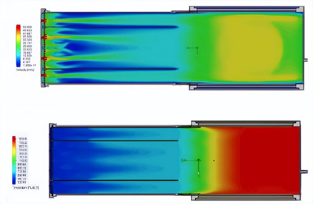
Figure 1 Simulated gas velocity magnitude (top) and gas temperature (bottom) in the PE1O8 process chamber at a plane located 10 mm above the substrate.
Other features include an improved gas rotation system that uses a feedback control algorithm to smooth the performance and directly measure the rotation speed, and a new generation of PID for temperature control. Epitaxy process parameters. An n-type 4H-SiC epitaxial growth process was developed in a prototype chamber. Trichlorosilane and ethylene were used as precursors for silicon and carbon atoms; H2 was used as carrier gas and nitrogen was used for n-type doping. Si-faced commercial 150mm SiC substrates and research-grade 200mm SiC substrates were used to grow 6.5μm thick 1×1016cm-3 n-doped 4H-SiC epilayers. The substrate surface was etched in situ using a H2 flow at elevated temperature. After this etching step, an n-type buffer layer was grown using a low growth rate and a low C/Si ratio to prepare a smoothing layer. On top of this buffer layer, an active layer with a high growth rate (30μm/h) was deposited using a higher C/Si ratio. The developed process was then transferred to a PE1O8 reactor installed at ST's Swedish facility. Similar process parameters and gas distribution were used for 150mm and 200mm samples. Fine tuning of growth parameters was postponed to future studies due to the limited number of available 200 mm substrates.
The apparent thickness and doping performance of the samples were evaluated by FTIR and CV mercury probe, respectively. The surface morphology was investigated by Nomarski differential interference contrast (NDIC) microscopy, and the defect density of the epilayers was measured by Candela. Preliminary results. Preliminary results of doping and thickness uniformity of 150 mm and 200 mm epitaxially grown samples processed in the prototype chamber are shown in Figure 2. The epilayers grew uniformly along the surface of the 150 mm and 200 mm substrates, with thickness variations (σ/mean) as low as 0.4% and 1.4%, respectively, and doping variations (σ-mean) as low as 1.1% and 5.6%. Intrinsic doping values were approximately 1×1014 cm-3.
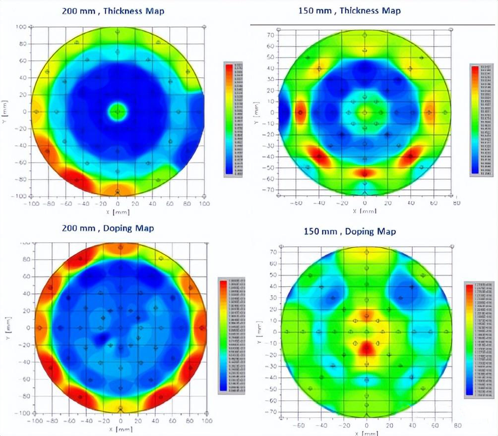
Figure 2 Thickness and doping profiles of 200 mm and 150 mm epiwafers.
The repeatability of the process was investigated by comparing run-to-run variations, resulting in thickness variations as low as 0.7% and doping variations as low as 3.1%. As shown in Figure 3, the new 200mm process results are comparable to the state-of-the-art results previously obtained on 150mm by a PE1O6 reactor.
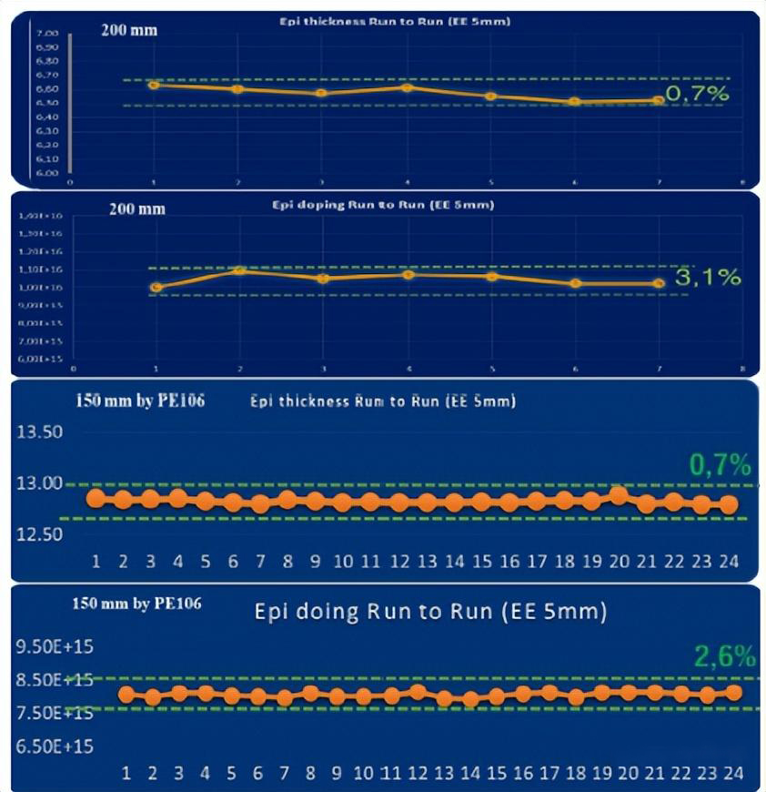
Figure 3 Layer-by-layer thickness and doping uniformity of a 200mm sample processed by a prototype chamber (top) and a state-of-the-art 150mm sample fabricated by PE1O6 (bottom).
Regarding the surface morphology of the samples, NDIC microscopy confirmed a smooth surface with roughness below the detectable range of the microscope. PE1O8 results. The process was then transferred to a PE1O8 reactor. The thickness and doping uniformity of the 200mm epiwafers are shown in Figure 4. The epilayers grow uniformly along the substrate surface with thickness and doping variations (σ/mean) as low as 2.1% and 3.3%, respectively.
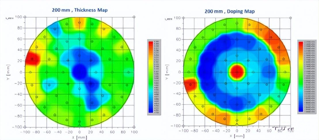
Figure 4 Thickness and doping profile of a 200mm epiwafer in a PE1O8 reactor.
To investigate the defect density of epitaxially grown wafers, candela was used. As shown in the figure. Total defect densities of 5 as low as 1.43 cm-2 and 3.06 cm-2 were achieved on the 150mm and 200mm samples, respectively. The total available area (TUA) after epitaxy was therefore calculated to be 97% and 92% for the 150mm and 200mm samples, respectively. It is worth mentioning that these results were achieved only after a few runs and can be further improved by fine-tuning the process parameters.
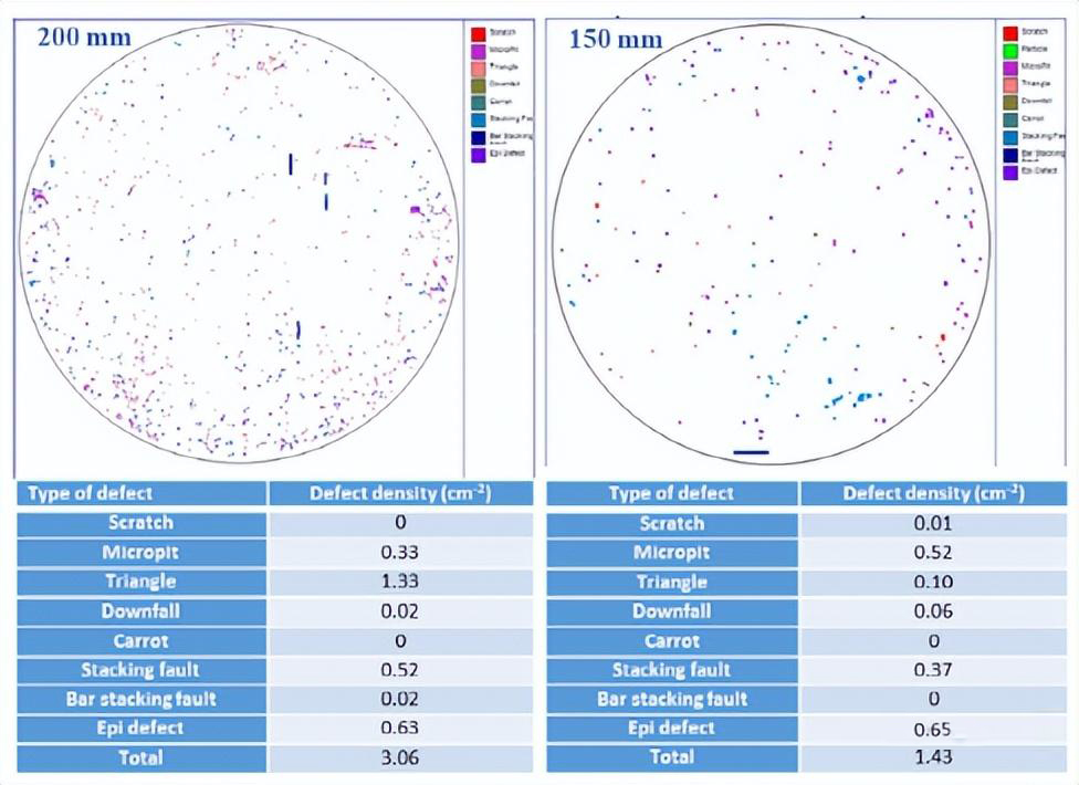
Figure 5 Candela defect maps of 6μm thick 200mm (left) and 150mm (right) epiwafers grown with PE1O8.
Conclusion
This paper presents the newly designed PE1O8 hot-wall CVD reactor and its ability to perform uniform 4H-SiC epitaxy on 200mm substrates. Preliminary results on 200mm are very promising, with thickness variations as low as 2.1% across the sample surface and doping performance variations as low as 3.3% across the sample surface. The TUA after epitaxy was calculated to be 97% and 92% for the 150mm and 200mm samples, respectively, and the TUA for 200mm is predicted to improve in the future with higher substrate quality. Considering that the results on 200mm substrates reported here are based on a few sets of tests, we believe that it will be possible to further improve the results, which are already close to the state-of-the-art results on 150mm samples, by fine-tuning the growth parameters.


