- English
- Español
- Português
- русский
- Français
- 日本語
- Deutsch
- tiếng Việt
- Italiano
- Nederlands
- ภาษาไทย
- Polski
- 한국어
- Svenska
- magyar
- Malay
- বাংলা ভাষার
- Dansk
- Suomi
- हिन्दी
- Pilipino
- Türkçe
- Gaeilge
- العربية
- Indonesia
- Norsk
- تمل
- český
- ελληνικά
- український
- Javanese
- فارسی
- தமிழ்
- తెలుగు
- नेपाली
- Burmese
- български
- ລາວ
- Latine
- Қазақша
- Euskal
- Azərbaycan
- Slovenský jazyk
- Македонски
- Lietuvos
- Eesti Keel
- Română
- Slovenski
- मराठी
- Srpski језик
What is the epitaxial process?
2024-12-23
Overview of Epitaxial Processes
The term "epitaxy" derives from the Greek words "epi," meaning "upon," and "taxis," meaning "ordered," indicating the ordered nature of the crystalline growth. Epitaxy is a crucial process in semiconductor fabrication, referring to the growth of a thin crystalline layer on a crystalline substrate. The epitaxy (epi) process in semiconductor fabrication aims to deposit a fine layer of single crystal, usually around 0.5 to 20 microns, on a single crystal substrate. The epi process is a significant step in semiconductor device manufacturing, especially in silicon wafer fabrication.
Epitaxy allows for the deposition of thin films that are highly ordered and can be tailored for specific electronic properties. This process is essential for creating high-quality semiconductor devices, such as diodes, transistors, and integrated circuits.
![]()
Types of Epitaxy
In the epitaxy process, the orientation of the growth is determined by the underlying base crystal. There can be either one or many epitaxy layers depending on the repetition of the deposition. The epitaxy process can be employed to form a thin layer of material that can be either the same or different from the underlying substrate in terms of chemical composition and structure. Epitaxy can be classified into two primary categories based on the relationship between the substrate and the epitaxial layer:Homoepitaxy and Heteroepitaxy.
Next, we will analyze the differences between Homoepitaxy and Heteroepitaxy from four dimensions: Grown layer, Crystal structure and lattice, Example, and Application:
● Homoepitaxy: This occurs when the epitaxial layer is made from the same material as the substrate.
✔ Grown layer: The epitaxially grown layer is of the same material as the substrate layer.
✔ Crystal structure and lattice: The crystal structure and lattice constant of the substrate and epitaxial layer are the same.
✔ Example: Epitaxial growth of highly pure silicon over substrate silicon.
✔ Application: Semiconductor device construction where layers of different doping levels are required or pure films on substrates that are less pure.
● Heteroepitaxy: This involves different materials being used for the layer and substrate, such as growing aluminum gallium arsenide (AlGaAs) on gallium arsenide (GaAs). Successful heteroepitaxy requires similar crystal structures between the two materials to minimize defects.
✔ Grown layer: The epitaxially grown layer is of a different material than the substrate layer.
✔ Crystal structure and lattice: The crystal structure and lattice constant of the substrate and epitaxial layer are different.
✔ Example: Epitaxially growing gallium arsenide on a silicon substrate.
✔ Application: Semiconductor device construction where layers of different materials are needed or to build a crystalline film of a material that is not available as a single crystal.
Factors Influencing the Epi Process in Semiconductor Fabrication:
✔ Temperature: Affects the epitaxy rate and epitaxial layer density. The temperature required for the epitaxy process is higher than room temperature, and the value depends on the type of epitaxy.
✔ Pressure: Affects the epitaxy rate and epitaxial layer density.
✔ Defects: Defects in the epitaxy lead to faulty wafers. The physical conditions required for the epi process should be maintained for non-defective epitaxial layer growth.
✔ Desired position: The epitaxial growth should be in the correct positions on the crystal. The regions that should be excluded from the epitaxial process should be properly filmed to prevent growth.
✔ Autodoping: As the epitaxy process is conducted at high temperatures, dopant atoms may be capable of bringing variations in the material.
Epitaxial Growth Techniques
There are several methods to perform the epitaxy process: liquid phase epitaxy, hybrid vapor phase epitaxy, solid phase epitaxy, atom layer deposition, chemical vapor deposition, molecular beam epitaxy, etc. Let’s compare the two epitaxy processes: CVD and MBE.
|
Chemical Vapor Deposition (CVD) |
Molecular Beam Epitaxy (MBE) |
|
Chemical process |
Physical process |
|
Involves a chemical reaction that takes place when gaseous precursors meet the heated substrate in the growth chamber or reactor |
The material to be deposited is heated under vacuum conditions |
|
Precise control over the film growth process |
Precise control over the thickness of the growth layer and composition |
|
Employed in applications requiring an epitaxial layer of high-quality |
Employed in applications requiring an extremely fine epitaxial layer |
|
Most commonly used method |
Expensive |
Epitaxial Growth Modes
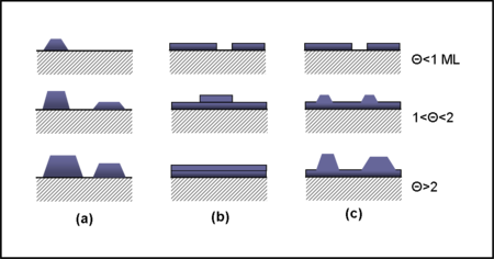
Epitaxy Growth Modes: Epitaxial growth can occur through different modes, which affect how layers form:

✔ (a) Volmer-Weber (VW): Characterized by three-dimensional island growth where nucleation occurs before continuous film formation.
✔ (b) Frank-Van der Merwe (FM): Involves layer-by-layer growth, promoting uniform thickness.
✔ (c) Stranski-Krastanov (SK): A combination of VW and FM, starting with layer growth that transitions into island formation after a critical thickness is reached.
Epitaxy Growth’s Importance in Semiconductor Manufacturing
Epitaxy is vital for enhancing the electrical properties of semiconductor wafers. The ability to control doping profiles and achieve specific material characteristics makes epitaxy indispensable in modern electronics.
Moreover, epitaxial processes are increasingly significant in developing high-performance sensors and power electronics, reflecting ongoing advancements in semiconductor technology. The precision required in controlling parameters such as temperature, pressure, and gas flow rate during epitaxial growth is critical for achieving high-quality crystalline layers with minimal defects.


