
- English
- Español
- Português
- русский
- Français
- 日本語
- Deutsch
- tiếng Việt
- Italiano
- Nederlands
- ภาษาไทย
- Polski
- 한국어
- Svenska
- magyar
- Malay
- বাংলা ভাষার
- Dansk
- Suomi
- हिन्दी
- Pilipino
- Türkçe
- Gaeilge
- العربية
- Indonesia
- Norsk
- تمل
- český
- ελληνικά
- український
- Javanese
- فارسی
- தமிழ்
- తెలుగు
- नेपाली
- Burmese
- български
- ລາວ
- Latine
- Қазақша
- Euskal
- Azərbaycan
- Slovenský jazyk
- Македонски
- Lietuvos
- Eesti Keel
- Română
- Slovenski
- मराठी
- Srpski језик
What measurement equipment are there in the Fab factory? - VeTek semiconductor
2024-11-25
There are many types of measurement equipment in the Fab factory. The following are some common equipment:
Photolithography process measurement equipment
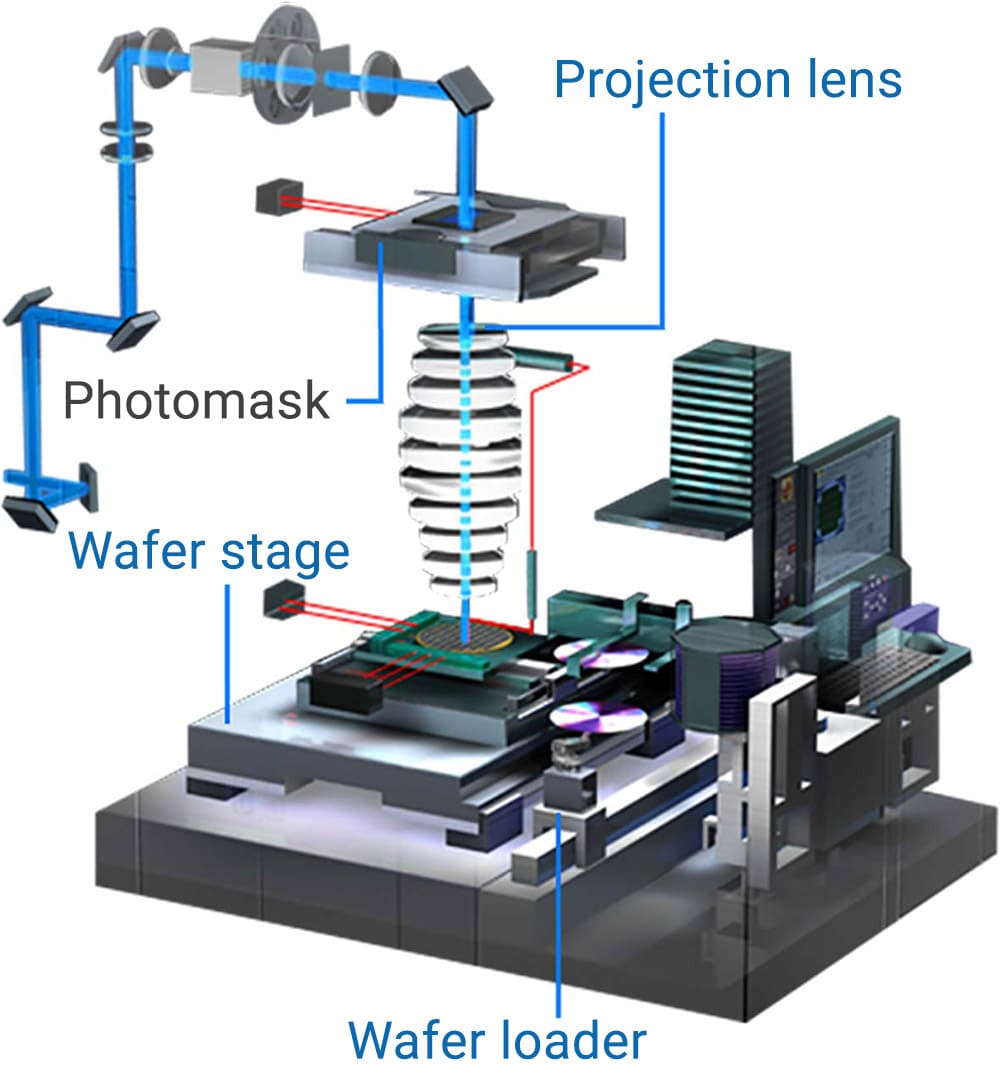
• Photolithography machine alignment accuracy measurement equipment: such as ASML's alignment measurement system, which can ensure the accurate superposition of different layer patterns.
• Photoresist thickness measurement instrument: including ellipsometers, etc., which calculate the thickness of photoresist based on the polarization characteristics of light.
• ADI t and AEI detection equipment: detect the photoresist development effect and pattern quality after photolithography, such as the relevant detection equipment of Vip Optoelectronics.
Etching process measurement equipment
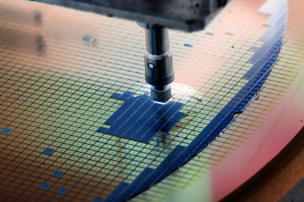
• Etching depth measurement equipment: such as white light interferometer, which can accurately measure the slight changes in etching depth.
• Etching profile measurement instrument: use electron beam or optical imaging technology to measure the profile information such as the side wall angle of the pattern after etching.
• CD-SEM: can accurately measure the size of microstructures such as transistors.
Thin film deposition process measurement equipment
• Film thickness measuring instruments: such as optical reflectometers, X-ray reflectometers, etc., can measure the thickness of various films deposited on the surface of the wafer.
• Film stress measuring equipment: By measuring the stress generated by the film on the wafer surface, the quality of the film and its potential impact on the wafer performance are judged.
Doping process measuring equipment
![]()
• Ion implantation dose measuring equipment: Determine the ion implantation dose by monitoring parameters such as beam intensity during ion implantation or performing electrical tests on the wafer after implantation.
• Doping concentration and distribution measuring equipment: For example, secondary ion mass spectrometers (SIMS) and spreading resistance probes (SRP) can measure the concentration and distribution of doping elements in the wafer.
CMP process measuring equipment
![]()
• Post-polishing flatness measuring equipment: Use optical profilometers and other equipment to measure the flatness of the wafer surface after polishing.
• Polishing removal measuring equipment: Determine the amount of material removed during polishing by measuring the depth or thickness change of a mark on the wafer surface before and after polishing.
Wafer particle detection equipment
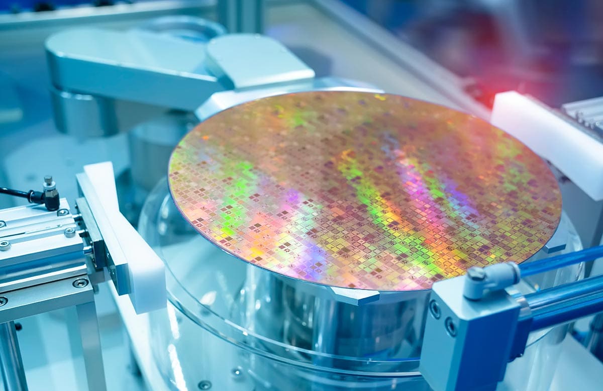
• KLA SP 1/2/3/5/7 and other equipment: can effectively detect particle contamination on the wafer surface.
• TORNADO series: TORNADO series equipment of Vip Optoelectronics can detect defects such as particles on the wafer, generate defect maps, and feedback to related processes for adjustment.
• ALFA-X intelligent visual inspection equipment: through the CCD-AI image control system, use displacement and visual sensing technology to distinguish wafer images and detect defects such as particles on the wafer surface.
Other measuring equipment
• Optical microscope: used to observe the microstructure and defects on the wafer surface.
• Scanning electron microscope (SEM): can provide higher resolution images for observing the microscopic morphology of the wafer surface.
• Atomic force microscope (AFM): can measure information such as the roughness of the wafer surface.
• Ellipsometer: in addition to measuring the thickness of photoresist, it can also be used to measure parameters such as the thickness and refractive index of thin films.
• Four-probe tester: used to measure electrical performance parameters such as the resistivity of the wafer.
• X-ray diffractometer (XRD): can analyze the crystal structure and stress state of wafer materials.
• X-ray photoelectron spectrometer (XPS): used to analyze the elemental composition and chemical state of the wafer surface.
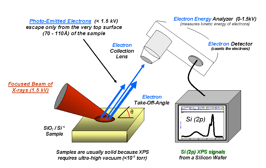
• Focused ion beam microscope (FIB): can perform micro-nano processing and analysis on wafers.
• Macro ADI equipment: such as Circle machine, used for macro detection of pattern defects after lithography.
• Mask defect detection equipment: detect defects on the mask to ensure the accuracy of the lithography pattern.
• Transmission electron microscope (TEM): can observe the microstructure and defects inside the wafer.
• Wireless temperature measurement wafer sensor: suitable for a variety of process equipment, measuring temperature accuracy and uniformity.


