- English
- Español
- Português
- русский
- Français
- 日本語
- Deutsch
- tiếng Việt
- Italiano
- Nederlands
- ภาษาไทย
- Polski
- 한국어
- Svenska
- magyar
- Malay
- বাংলা ভাষার
- Dansk
- Suomi
- हिन्दी
- Pilipino
- Türkçe
- Gaeilge
- العربية
- Indonesia
- Norsk
- تمل
- český
- ελληνικά
- український
- Javanese
- فارسی
- தமிழ்
- తెలుగు
- नेपाली
- Burmese
- български
- ລາວ
- Latine
- Қазақша
- Euskal
- Azərbaycan
- Slovenský jazyk
- Македонски
- Lietuvos
- Eesti Keel
- Română
- Slovenski
- मराठी
- Srpski језик
Semiconductor process: Chemical Vapor Deposition (CVD)
2024-11-07
In semiconductors and FPD panel displays, the preparation of thin films is an important process. There are many ways to prepare thin films (TF, Thin Film), the following two methods are common:
● CVD (Chemical Vapor Deposition)
● PVD (Physical Vapor Deposition)
Among them, the buffer layer/active layer/insulating layer are all deposited in the chamber of the machine using PECVD.
● Use special gases: SiH4/NH3/N2O for the deposition of SiN and Si/SiO2 films.
● Some CVD machines need to use H2 for hydrogenation to increase carrier mobility.
● NF3 is a cleaning gas. In comparison: F2 is highly toxic, and the greenhouse effect of SF6 is higher than that of NF3.
In the semiconductor device process, there are more types of thin films, in addition to the common SiO2/Si/SiN, there are also W, Ti/TiN, HfO2, SiC, etc.
This is also the reason why there are many kinds of precursors for advanced materials used in the semiconductor industry, in order to make various types of thin films.
We explain it in the following way:
1. Types of CVD and some precursor gases
2. Basic mechanism of CVD and film quality
1. Types of CVD and some precursor gases
CVD is a very general concept and can be divided into many types. Common ones are:
● PECVD: Plasma Enhanced CVD
● LPCVD: Low Pressure CVD
● ALD: Atomic Layer Deposition
● MOCVD: Metal-organic CVD
During the CVD process, the chemical bonds of the precursor need to be broken before chemical reactions.
The energy for breaking chemical bonds comes from heat, so the chamber temperature will be relatively high, which is not friendly to some processes, such as the substrate glass of the panel or the PI material of the flexible screen. Therefore, by inputting other energy (forming Plasma, etc.) to reduce the process temperature to meet some processes that require temperature, the thermal budget will also be reduced.
Therefore, PECVD deposition of a-Si:H/SiN/poly-Si is widely used in the FPD display industry. Common CVD precursors and films:
Polycrystalline silicon/single crystal silicon SiO2 SiN/SiON W/Ti WSi2 HfO2/SiC
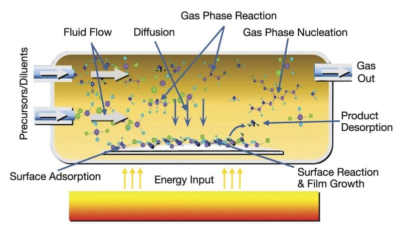
Steps of the basic mechanism of CVD:
1. Reaction precursor gas enters the chamber
2. Intermediate products produced by gas reaction
3. The intermediate products of the gas diffuse to the substrate surface
4. Adsorbed on the substrate surface and diffused
5. Chemical reaction occurs on the substrate surface, nucleation/island formation/film formation
6. Byproducts are desorbed, vacuum pumped away and discharged after entering the scrubber for treatment
As mentioned earlier, the whole process includes multiple steps such as diffusion/adsorption/reaction. The overall film formation rate is affected by many factors, such as temperature/pressure/type of reaction gas/type of substrate. Diffusion has a diffusion model for prediction, adsorption has an adsorption theory, and chemical reaction has a reaction kinetics theory.
In the whole process, the slowest step determines the entire reaction rate. This is very similar to the critical path method of project management. The longest activity flow determines the shortest project duration. The duration can be shortened by allocating resources to reduce the time of this path. Similarly, CVD can find the key bottleneck that limits the film formation rate by understanding the entire process, and adjust the parameter settings to achieve the ideal film formation rate.

2. Evaluation of CVD film quality
Some films are flat, some are hole filling, and some are groove filling, with very different functions. Commercial CVD machines must meet basic requirements:
● Machine processing capacity, deposition rate
● Consistency
● Gas phase reactions cannot produce particles. It is very important not to produce particles in the gas phase.
Some other evaluation requirements are as follows:
● Good step coverage
● Ability to fill high aspect ratio gaps (conformality)
● Good thickness uniformity
● High purity and density
● High degree of structural perfection with low film stress
● Good electrical properties
● Excellent adhesion to the substrate material


