
- English
- Español
- Português
- русский
- Français
- 日本語
- Deutsch
- tiếng Việt
- Italiano
- Nederlands
- ภาษาไทย
- Polski
- 한국어
- Svenska
- magyar
- Malay
- বাংলা ভাষার
- Dansk
- Suomi
- हिन्दी
- Pilipino
- Türkçe
- Gaeilge
- العربية
- Indonesia
- Norsk
- تمل
- český
- ελληνικά
- український
- Javanese
- فارسی
- தமிழ்
- తెలుగు
- नेपाली
- Burmese
- български
- ລາວ
- Latine
- Қазақша
- Euskal
- Azərbaycan
- Slovenský jazyk
- Македонски
- Lietuvos
- Eesti Keel
- Română
- Slovenski
- मराठी
- Srpski језик
Principles and Technology of Physical Vapor Deposition (PVD) Coating (2/2) - VeTek Semiconductor
2024-09-24
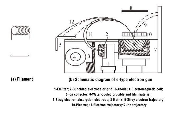
Electron beam evaporation coating
Due to some disadvantages of resistance heating, such as low energy density provided by resistance evaporation source, certain evaporation of evaporation source itself affecting film purity, etc., new evaporation sources need to be developed. Electron beam evaporation coating is a coating technology that puts the evaporation material into a water-cooled crucible, directly uses electron beam to heat the film material, and vaporizes the film material and condenses it on the substrate to form a film. Electron beam evaporation source can be heated to 6000 degrees Celsius, which can melt almost all common materials, and can deposit thin films on substrates such as metals, oxides and plastics at high speed.
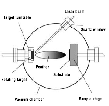
Laser pulse deposition
Pulsed laser deposition (PLD) is a film-making method that uses high-energy pulsed laser beam to irradiate target material (bulk target material or high-density bulk material pressed from powdered film material), so that the local target material rises to a very high temperature in an instant and vaporizes, forming a thin film on the substrate.
Molecular beam epitaxy
Molecular beam epitaxy (MBE) is a thin film preparation technology that can accurately control the thickness of epitaxial film, doping of thin film and interface flatness at the atomic scale. It is mainly used to prepare high-precision thin films for semiconductors such as ultra-thin films, multi-layer quantum wells and superlattices. It is one of the main preparation technologies for the new generation of electronic devices and optoelectronic devices.
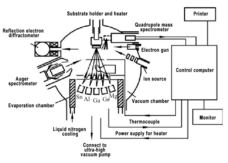
Molecular beam epitaxy is a coating method that places the components of the crystal in different evaporation sources, slowly heats the film material under ultra-high vacuum conditions of 1e-8Pa, forms a molecular beam flow, and sprays it onto the substrate at a certain thermal motion speed and a certain proportion, grows epitaxial thin films on the substrate, and monitors the growth process online.
In essence, it is a vacuum evaporation coating, including three processes: molecular beam generation, molecular beam transport and molecular beam deposition. The schematic diagram of the molecular beam epitaxy equipment is shown above. The target material is placed in the evaporation source. Each evaporation source has a baffle. The evaporation source is aligned with the substrate. The substrate heating temperature is adjustable. In addition, there is a monitoring device to monitor the crystalline structure of the thin film online.
Vacuum sputtering coating
When the solid surface is bombarded with energetic particles, the atoms on the solid surface are collided with the energetic particles, and it is possible to obtain sufficient energy and momentum and escape from the surface. This phenomenon is called sputtering. Sputtering coating is a coating technology that bombards solid targets with energetic particles, sputtering target atoms and depositing them on the substrate surface to form a thin film.
Introducing a magnetic field on the cathode target surface can use the electromagnetic field to constrain electrons, extend the electron path, increase the probability of ionization of argon atoms, and achieve stable discharge under low pressure. The coating method based on this principle is called magnetron sputtering coating.
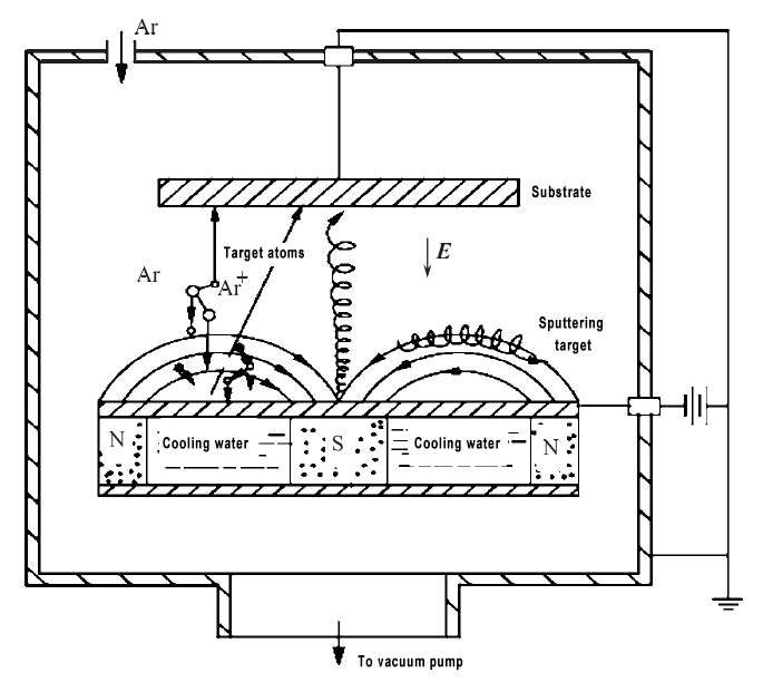
The principle diagram of DC magnetron sputtering is as shown above. The main components in the vacuum chamber are the magnetron sputtering target and the substrate. The substrate and the target are facing each other, the substrate is grounded, and the target is connected to a negative voltage, that is, the substrate has a positive potential relative to the target, so the direction of the electric field is from the substrate to the target. The permanent magnet used to generate the magnetic field is set on the back of the target, and the magnetic lines of force point from the N pole of the permanent magnet to the S pole, and form a closed space with the cathode target surface.
The target and the magnet are cooled by cooling water. When the vacuum chamber is evacuated to less than 1e-3Pa, Ar is filled into the vacuum chamber to 0.1 to 1Pa, and then a voltage is applied to the positive and negative poles to make the gas glow discharge and form plasma. The argon ions in the argon plasma move toward the cathode target under the action of the electric field force, are accelerated when passing through the cathode dark area, bombard the target, and sputter out target atoms and secondary electrons.
In the DC sputtering coating process, some reactive gases are often introduced, such as oxygen, nitrogen, methane or hydrogen sulfide, hydrogen fluoride, etc. These reactive gases are added to the argon plasma and are excited, ionized or ionized together with the Ar atoms to form a variety of active groups. These activated groups reach the surface of the substrate together with the target atoms, undergo chemical reactions, and form corresponding compound films, such as oxides, nitrides, etc. This process is called DC reactive magnetron sputtering.
VeTek Semiconductor is a professional Chinese manufacturer of Tantalum Carbide Coating, Silicon Carbide Coating, Special Graphite, Silicon Carbide Ceramics and Other Semiconductor Ceramics. VeTek Semiconductor is committed to providing advanced solutions for various Coating products for the semiconductor industry.
If you have any inquiries or need additional details, please don't hesitate to get in touch with us.
Mob/WhatsAPP: +86-180 6922 0752
Email: anny@veteksemi.com


